
When Purchasing a New Electronic Device You Should Consider
Introduction: The Critical Choice of Selecting New Electronics When it comes to purchasing new electronic devices, consumers are faced with a myriad of options. Each
Introduction: The Critical Choice of Selecting New Electronics When it comes to purchasing new electronic devices, consumers are faced with a myriad of options. Each
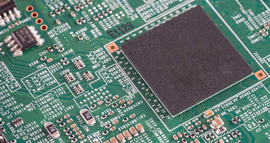
Introduction to PCB Manufacturability Printed Circuit Board (PCB) manufacturability refers to the ease and efficiency with which PCBs can be manufactured. It’s a crucial aspect

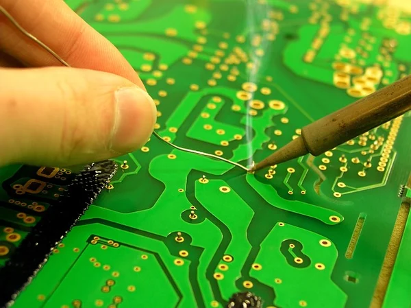
Introduction to PCB Printing Printed Circuit Board (PCB) printing involves translating a design schematic into a physical board that connects electronic components. This process is
Understanding the cost of circuit boards is crucial for anyone involved in electronics, whether you’re a hobbyist, an engineer, or a business looking to manufacture
What is PCB Corrosion? PCB corrosion is when the metal parts on a printed circuit board (PCB) start to deteriorate due to exposure to moisture

Introduction to PCB and Multimeters Printed Circuit Boards (PCBs) are the backbone of most electronic devices. They support electronic components and connect them through conductive
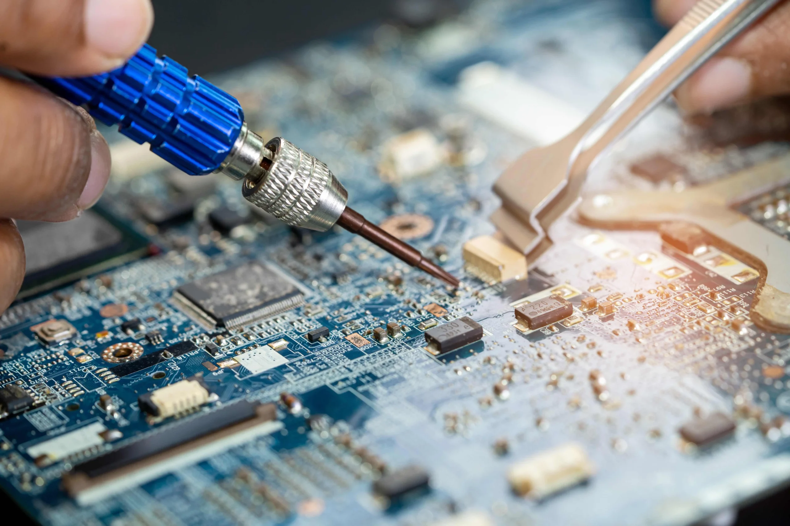
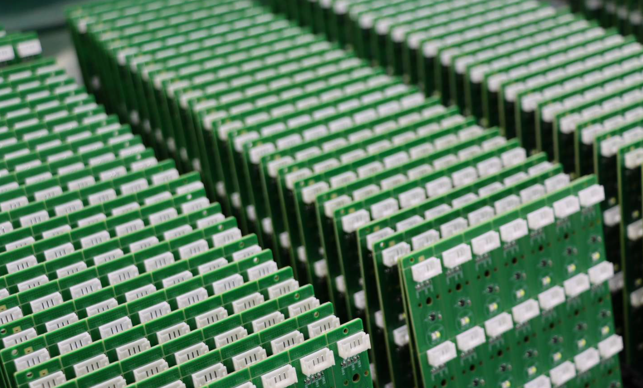
Introduction to Electronic Board Manufacturing Electronic board manufacturing is a high-precision process that involves the complex assembly of electronic components onto printed circuit boards (PCBs).
Overview Selecting the appropriate PCB stackup is a critical step in designing a printed circuit board (PCB) that meets your performance, reliability, and cost requirements.

Introduction to PCB Manufacturing and Assembly Printed Circuit Board (PCB) manufacturing and assembly is a complex process that involves creating boards to connect electronic components.
Introduction to MCPCB and Its Importance in PCB Design Metal Core Printed Circuit Boards (MCPCBs) are pivotal in managing heat dissipation for electronic components. They

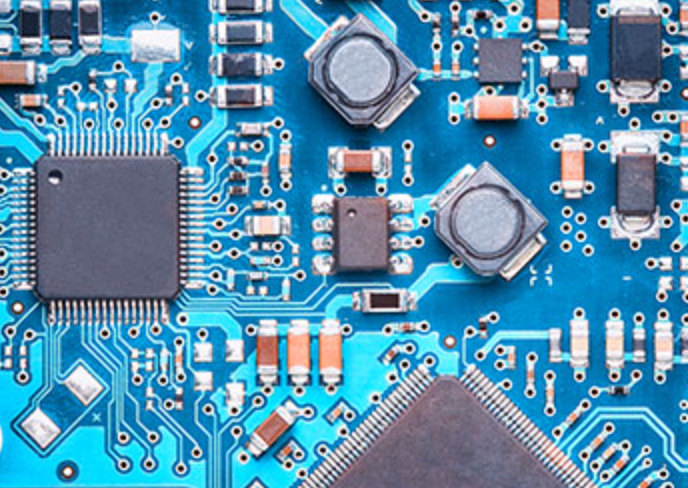
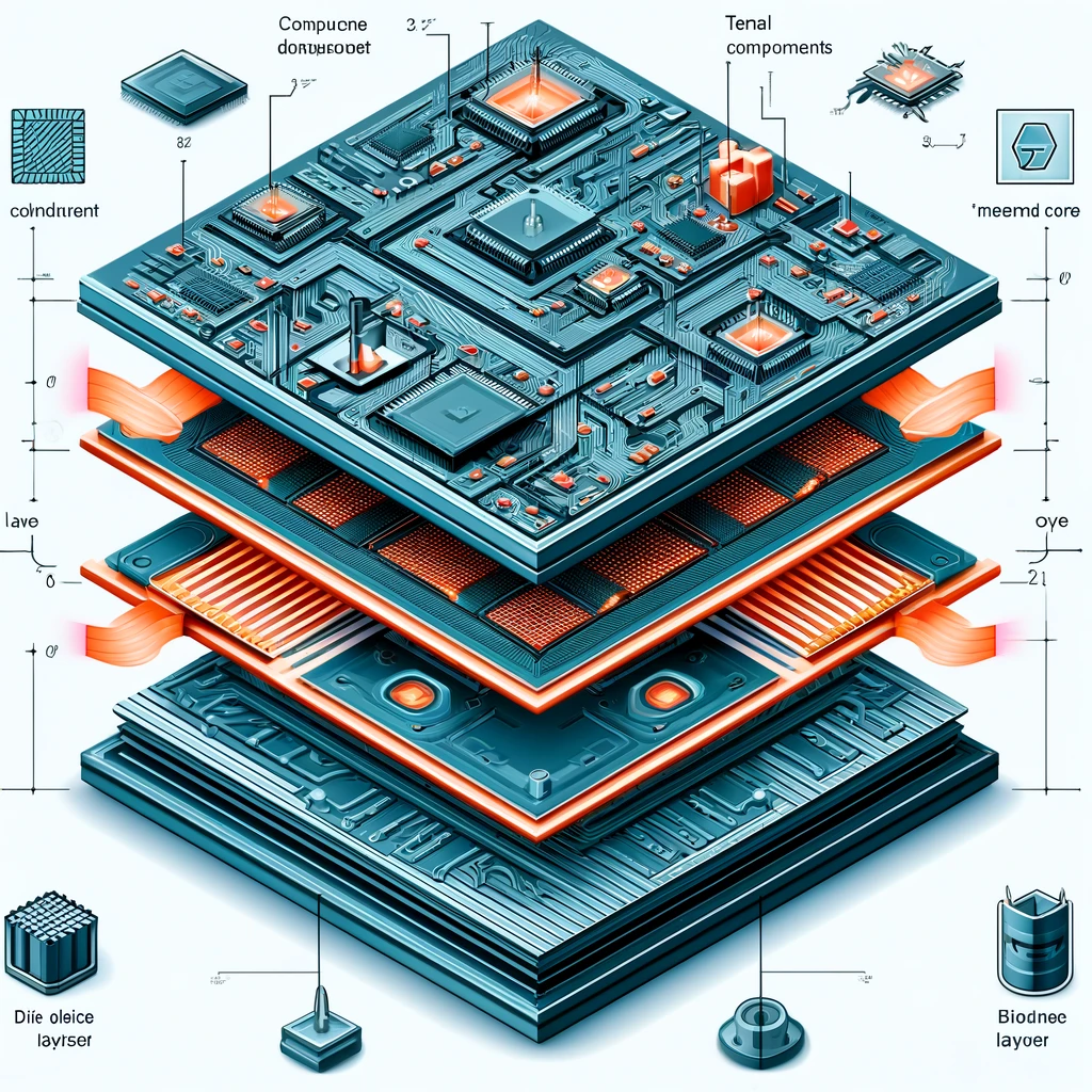
The construction of Printed Circuit Boards (PCBs) is a complex process that involves multiple layers, each with specific functionalities that contribute to the board’s electrical
In the fast-paced world of electronic product development, the speed at which a prototype can be turned from a concept into a tangible product is