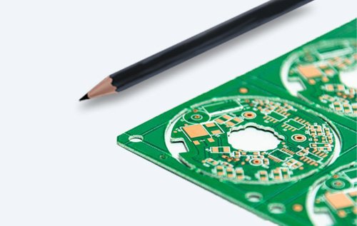
PCB Design services
At Arisentec Tech,the best pcb manufacturer in China, we specialize in delivering quick turn PCB prototypes, ensuring that our clients can swiftly move from conceptualization to realization. Our printed circuit board prototype services are designed to meet the highest standards of quality and precision. Recognized for our fast PCB prototyping service, we have become the go-to choice for engineers and developers working on intricate PCB board projects. Our commitment is to provide unparalleled speed without compromising on the integrity and functionality of the final product.


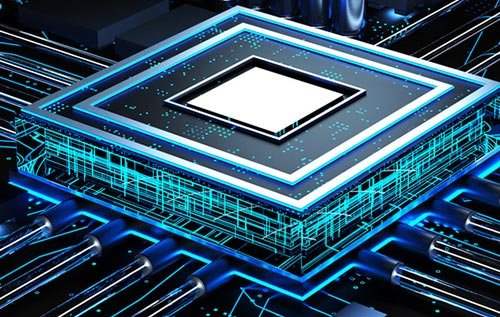
What is “PCB Design”
PCB design refers to the process of designing a Printed Circuit Board (PCB). This involves several steps to ensure the board efficiently and reliably connects all the electronic components in a device.
Key aspects of PCB design include:
Schematic Design: Creating a schematic or diagram that shows all the components and their connections. This is a conceptual representation of the circuit.
Board Layout: Translating the schematic into a physical layout that determines the placement of components and the routing of electrical traces on the PCB.
Material Selection: Choosing the appropriate materials for the PCB, considering factors like thermal performance, electrical insulation, and durability.
Layer Planning: For complex circuits, multiple layers of conductive traces might be needed. Deciding on the number of layers and their arrangement is a crucial step.
Trace Routing: Designing the path of electrical connections (traces) on the board to connect different components, while minimizing interference and signal loss.
Component Placement: Strategically placing components to optimize the board’s performance and to ensure ease of manufacturing.
Testing and Validation: Simulating the PCB design to check for potential issues like short circuits, signal integrity problems, or electromagnetic interference.
Manufacturing File Preparation: Creating detailed instructions and files for manufacturing the PCB, including specifications for drilling, plating, and other fabrication processes.

- DDRx, LPDDRx, GDDRx
- PCIe Gen 3, Gen 4, Gen 5
- SAS-3, SAS-4
- Infiniband
- 1Gb and 10Gb Ethernet
- Thunderbolt 2, Thunderbolt 3
- SFP28, QSFP28
- FPGA, DSP, Programmable SoCs
PCB DESIGN SERVICE
quick turn pcb prototypes

Consulting