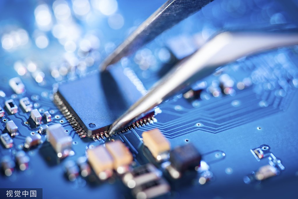
- Introduction to PCB Manufacturability
- Understanding the Interplay between Mechanical Design and Electrical Performance
- Key Mechanical Design Considerations for PCB Layout
- The Importance of Dimensional Tolerances in PCB Design
- Design for Assembly (DFA) Principles in PCB Manufacturing
- Optimizing PCB Design for Automated Assembly Processes
- Thermal Management and Mechanical Design Strategies
- Incorporating Flexibility in Mechanical Designs for Future Upgrades
- Mitigating Electromechanical Interferences in PCB Assemblies
- The Role of 3D Modeling in Enhancing PCB Manufacturability
- Ensuring Compliance with Industry Standards in Mechanical PCB Design
- Testing and Prototyping: Validating Mechanical Design Choices
- Conclusion: The Integral Role of Mechanical Design in PCB Development
Introduction to PCB Manufacturability
Printed Circuit Board (PCB) manufacturability refers to the ease and efficiency with which PCBs can be manufactured. It’s a crucial aspect of the PCB design process and involves making choices that anticipate potential production issues. Good manufacturability practices ensure that the PCB design is optimized for:
l Cost-effective production
l High yield rates
l Consistency in quality
l Suitable performance in the intended application
l Ease of assembly during the next stages of production
It is the mechanical design’s responsibility to accommodate electrical components while considering physical constraints and assembly processes.
In an era where technology integrates seamlessly into every aspect of our lives, choosing the right PCB manufacturer becomes crucial. Companies like Arisentec, renowned as one of the best PCB manufacturers in China, provide comprehensive solutions from PCB design services to quick turn PCB prototypes.
Understanding the Interplay between Mechanical Design and Electrical Performance
In PCB manufacturing, mechanical design critically affects electrical performance. The layout of traces, spacing, and component placement can influence signal integrity, power distribution, and electromagnetic compatibility (EMC). To optimize performance:
l Adequately space traces to reduce crosstalk and improve signal integrity.
l Design robust via structures to ensure reliable electrical connections.
l Implement proper grounding and shielding techniques to enhance EMC.
l Consider the thermal management through strategic component placement and heat sink integration.
These mechanical considerations can prevent performance degradation and ensure long-term reliability of the electrical assembly.
Key Mechanical Design Considerations for PCB Layout
Component Placement: Factor in heat dissipation and electromagnetic compatibility when positioning components to enhance reliability and performance.
Trace Routing: Plan traces to minimize cross-talk and impedance issues, respecting signal integrity and power distribution needs.
Board Size and Shape: Design for the enclosure, considering constraints and mounting requirements to ensure the PCB fits properly.
Thermal Management: Integrate heat sinks, cooling vias, and thermal relief pads to manage hot spots and improve overall device longevity.
Flex and Rigidity: If using flexible PCBs, account for bend ratios and stress points to prevent circuit failure.
Stack-Up: Choose a suitable number of layers and material thickness to meet electrical needs while considering manufacturability and cost efficiency.
Assembly and Serviceability: Design for straightforward assembly and repair, including adequate spacing for soldering and component replacement.
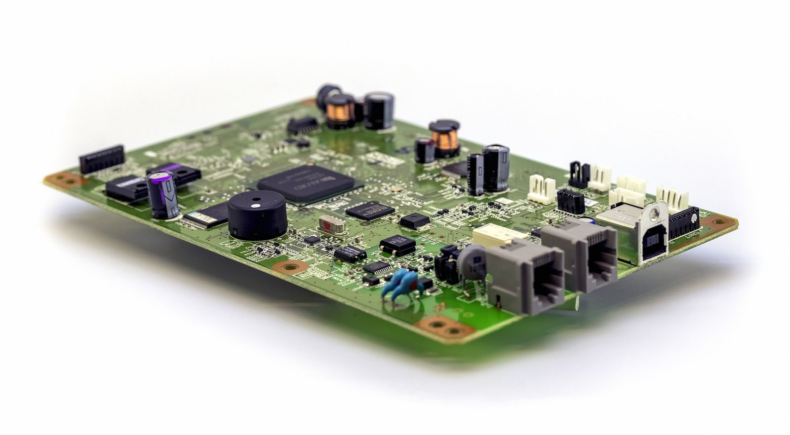
Material Selection for Reliability and Manufacturability
Choosing the right materials for printed circuit boards (PCBs) is critical for both reliability and manufacturability. Designers must consider several factors:
Thermal Management: Materials must withstand the operational temperature range without degrading.
Mechanical Strength: The chosen substrate should provide enough rigidity and flexibility to endure handling and use.
Electrical Properties: Dielectric constants and loss tangents influence signal integrity; materials should minimize electrical noise.
Chemical Resistance: Exposure to solvents during manufacturing and operation demands chemically robust materials.
Manufacturing Compatibility: Materials should be amenable to standard PCB manufacturing processes to prevent increased costs or extended timelines.
Selecting materials that meet these criteria ensures a PCB design that is both reliable and manufacturable.
The Importance of Dimensional Tolerances in PCB Design
Dimensional tolerances are critical in PCB design, ensuring parts fit accurately, mitigating the risk of assembly issues. Tight tolerances lead to consistent electrical performance, while overly strict tolerances can increase costs without added benefits. Properly set tolerances:
Facilitate smooth assembly line operation by preventing mechanical fit problems.
Reduce the requirement for manual rework, saving time and resources.
Enhance the reliability of the final product, as components align with intended design specifications.
Allow for appropriate clearances and creepage distances, essential for safety and functionality in electrical circuits.
Choosing the right balance is crucial for optimizing manufacturability and functionality.
Design for Assembly (DFA) Principles in PCB Manufacturing
Design for Assembly (DFA) principles enhance PCB manufacturability by simplifying assembly processes and reducing costs. Key DFA principles include:
Minimizing Part Count: By reducing the number of components, assembly time is decreased, and potential failure points are minimized.
Standardizing Components and Processes: Utilizing common parts and assembly techniques simplifies production and maintenance.
Designing for Automated Assembly: Creating PCB layouts compatible with automated assembly machinery increases speed and consistency.
Ease of Insertion: Orientation and placement of parts should allow for clear assembly paths to reduce the risk of damage.
Modular Design: Segmenting the PCB into modules can streamline testing and replacement, facilitating repairs and upgrades.
When considering PCB assembly and PCBA manufacture, it’s essential to partner with providers who offer not just expertise but also versatility. Arisentec, a leader in printed circuit board assembly, offers turnkey PCB assembly services that streamline the development process from conception to production, ensuring a quick and efficient project turnaround.
Optimizing PCB Design for Automated Assembly Processes
To enhance PCB manufacturability for automated assembly, designers must prioritize several factors. First, component placements should follow a uniform orientation, simplifying machine handling. Second, maintaining a consistent clearance between components prevents assembly errors. Using standard component packages whenever possible also streamlines the automation process.
To further optimize for automation:
Select through-hole components judiciously, as surface-mount technology (SMT) is more automation-friendly.
Avoid placing heat-sensitive parts near high-temperature zones caused by reflow soldering processes.
Implement fiducial marks to improve the precision of component placement by automated systems.
Ensure that all labeling is machine-readable, favoring clear, consistent fonts and sizes.
Integrate a robust panelization strategy that accounts for the robotic handling and support of PCBs during the assembly.
Adhering to these guidelines helps reduce manufacturing time, costs, and the risk of errors, enabling a smooth transition from design to production.
Thermal Management and Mechanical Design Strategies
Effective thermal management is crucial in PCB manufacturing, with heat dissipation directly impacting performance and longevity. Designers must consider:
Heat sinks: Implementing these components to absorb and disperse heat.
Thermal vias: Placing these pathways to transfer heat from hot spots to a cooler place.
Material choice: Opting for materials with higher thermal conductivity.
Additionally, mechanical design plays a pivotal role in manufacturability:
Component layout: Strategically arranging parts to minimize stress and avoid mechanical conflicts.
Structural supports: Incorporating braces or mounts for added rigidity.
Design for Assembly (DFA): Streamlining the design for efficient assembly, reducing errors and costs.
Incorporating Flexibility in Mechanical Designs for Future Upgrades
Designing PCB assemblies with future upgrades in mind ensures longevity and adaptability. To achieve this, mechanical engineers should:
Use modular components that can be easily replaced or expanded.
Provide extra space on the PCB for potential additions.
Select connectors that support higher bandwidths to accommodate future technologies.
Implement standardized mounting holes to allow for diverse component compatibility.
Design enclosures with adjustable fittings to ease hardware modifications.
By integrating these strategies, PCB assemblies can be seamlessly updated, aligning with evolving technological advancements and market needs.
Mitigating Electromechanical Interferences in PCB Assemblies
To reduce electromechanical interferences in PCB assemblies, focused tactics can significantly enhance performance:
Shielding: Implement metallic shields to block electromagnetic fields.
Grounding: Design robust ground planes to minimize noise and interference.
Routing: Route critical signals away from potential interference sources.
Separation: Keep analog and digital circuits separate to prevent crosstalk.
Component Placement: Position sensitive components strategically to mitigate effects from motors or transformers.
Filtering: Incorporate filters and transient voltage suppressors to protect against spikes.
Mechanical Design: Use precision in mechanical design to ensure tight and secure component fits that resist vibrations.
Standards Compliance: Adhere to industry standards, such as IPC guidelines, for layout and spacing.
Integrating these approaches during the design phase helps maintain signal integrity and functionality.
The Role of 3D Modeling in Enhancing PCB Manufacturability
3D modeling serves as a critical tool in the PCB design process by providing a comprehensive visualization of the final product before it enters production. It allows for:
l The detection of potential spatial conflicts and interferences within a PCB assembly, preventing issues that could arise from component overcrowding.
l Simulation of the PCB within its intended environment, ensuring compatibility with enclosures and other hardware.
l Streamlined communication amongst design team members and between designers and manufacturers, reducing the chances for misunderstandings and errors.
l Generation of accurate and detailed documentation that facilitates a more efficient manufacturing process.
l Implementation of design adjustments early in the development cycle, which minimizes costly revisions and enhances overall manufacturability.
3D modeling thereby significantly contributes to a more reliable, efficient, and cost-effective PCB manufacturing process.
Ensuring Compliance with Industry Standards in Mechanical PCB Design
Mechanical design in PCB fabrication plays a crucial role in adhering to industry standards. It’s fundamental that designers:
l Understand and apply relevant specifications, such as IPC-2221A, to ensure proper clearance, spacing, and material selection.
l Incorporate DFM (Design for Manufacturability) guidelines to minimize production issues and fulfill quality requirements.
l Regularly update their knowledge of industry changes, such as advancements in HDI (High-Density Interconnect) technologies.
l Ensure compatibility with assembly and testing fixtures, which often have strict dimensional and tolerance standards.
l Verify that mechanical enclosures accommodate the PCB without stress or interference, avoiding any potential reliability issues.
Testing and Prototyping: Validating Mechanical Design Choices
In optimizing PCB manufacturability, mechanical design plays a pivotal role. Thorough testing and prototyping become essential to validate mechanical design choices. During this phase:
l Finite Element Analysis (FEA) simulates physical stresses on components to predict failures.
l Rapid prototyping, such as 3D printing, facilitates physical examination of mechanical fits and clearances.
l Thermal testing ensures that heat dissipation is efficient and within design specifications, preventing overheating.
l Vibration and shock testing replicate operating conditions to ensure durability and longevity of the product under stress.
l Compliance with industry standards, such as IPC-2221, validates that design choices meet essential criteria for safety and functionality.
These tests confirm that the mechanical design aligns with electrical performance, ensuring a robust and reliable PCB assembly.
Conclusion: The Integral Role of Mechanical Design in PCB Development
Mechanical design is paramount in optimizing printed circuit board (PCB) manufacturability. It ensures that PCBs fit within their enclosures, interface seamlessly with their mechanical environment, and satisfy thermal management requirements. Additionally, it addresses manufacturability issues early on, reducing rework and ensuring that electrical assemblies are reliable, cost-effective, and ready for mass production. By integrating mechanical design considerations throughout the PCB development process, one can significantly improve the overall quality and performance of electronic products.
As the demand for sophisticated electronic components grows, so does the need for the best PCB manufacturers. Arisentec stands out not just in China but globally, offering tailored PCB solutions that cater to diverse industry needs. Whether it’s PCBA manufacturing or developing a printed circuit board prototype, Arisentec’s dedicated approach ensures that your projects are not just completed, but masterfully executed.

Choosing the Right Wires for Breadboard Wiring: A Comprehensive Guide
Breadboards are a staple in electronic circuit building, offering flexibility and ease of use for both beginners and professionals. However, one of the most critical aspects of working with breadboards is selecting the right wires. The wires you choose can impact not only the functionality of your circuit but also its longevity and ease of…

How to Improve Heat Dissipation in PCB Design
Introduction As modern electronic devices become more complex and power-dense, heat dissipation has emerged as a critical factor that directly impacts device performance and reliability. Excessive junction temperatures in electronic systems can shorten the lifespan of components and lead to system failure. Thus, optimizing the PCB (Printed Circuit Board) design to improve heat dissipation is…

Manufacturing Process of Multilayer PCBs
Multilayer PCB manufacturing methods include the plated-through hole (PTH) and high-density interconnect (HDI) methods, both achieved by combining different processes to realize the circuit board structure. Currently, the most widely used method is the PTH method, which has been developed and refined over more than half a century. The PTH method is mature in terms…