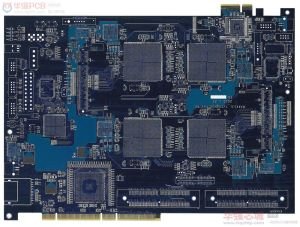
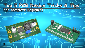
Blog

Your blog category

PCB Design Tips

PCB Design Tips

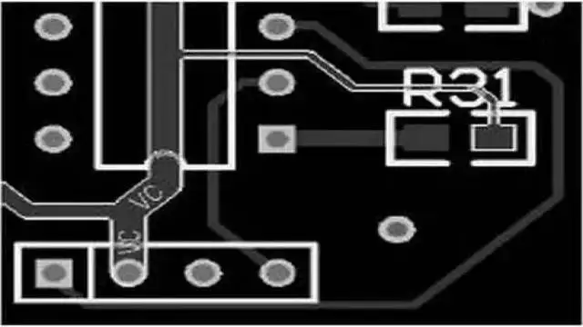
Preliminary preparation—PCB structure design—PCB layout—wiring—wiring optimization and silk screen printing—network and DRC inspection and structural inspection—plate making. 1. Preliminary preparations include the preparation of component libraries and schematic diagrams“If a worker wants to be good at his work, he must first sharpen his tools.” To make a good board, in addition to designing the principles …

PCB Design Tips Read More »

PCB Design Hole spacing cannot be ignored

In the production of single-sided or double-sided PCBs, the non-conducting holes or conducting holes are directly drilled after blanking; the multi-layer boards are drilled after the pressing board is completed.According to the function, drilling can be divided into: part hole, tool hole, through hole, blind hole, buried hole. Conventional drilling is processed by drilling machinery. …

PCB Design Hole spacing cannot be ignored Read More »

XXX-LPDDR4 SI And Timing Simulation Report

XXX-LPDDR4 SI And Timing Simulation Report

CONTENTS 01  Conclusion 02    Summary 03    Simulation Condition 04    Clock Signal Analysis 05    Address/CMD Signal Analysis 06    DQ/DM/DQS Signal Analysis – Write 07    DQ/DM/DQS Signal Analysis – Read 08   Reference Conclusion This design could not run to 3732Mbps, which is limited by the branch length on ADDR/DQ nets. Lpddr4 uses different VREF and termination(ODT) strategies …

XXX-LPDDR4 SI And Timing Simulation Report Read More »

Get a Free Quote