CONTENTS
01 Conclusion
02 Summary
03 Simulation Condition
04 Clock Signal Analysis
05 Address/CMD Signal Analysis
06 DQ/DM/DQS Signal Analysis – Write
07 DQ/DM/DQS Signal Analysis – Read
08 Reference
Conclusion
This design could not run to 3732Mbps, which is limited by the branch length on ADDR/DQ nets. Lpddr4 uses different VREF and termination(ODT) strategies (then DDR3/4) and not adapt to this long branch.
Modify the structure to reduce the branch length or put the LPDDR4 components on Top/Bottom back-to-back to short the branch, will improve the performance.
Summary
Signals | Action | CPU | LPDDR4 DRAM | |
Buffer Model | Buffer Model | Pass/Fail | ||
DDR_CK DDR_CK_N | Write | lpddr4_ocd_40p_40n_diff | CLK_INPUT_ODT80_VOH30_4266 | Pass |
DDR_A[5:0] DDR_ATB[1:0] DDR_CAL | Write | lpddr4_ocd_40p_40n | CA_INPUT_ODT80_VOH30_4266 | Fail |
DDR_CS_N[4:0] DDR_CKE[1:0] | Write | lpddr4_ocd_40p_40n | CS_INPUT_ODT80_VOH30_4266 | Pass |
DDR_DQS[3:0] DDR_DQS_N[3:0] DDR_DQ[31:0] DDR_DM[3:0] | Write | lpddr4_ocd_40p_40n_diff lpddr4_ocd_40p_40n | DQS_IN_ODT40_VOH30_4266 DQ_IN_ODT40_VOH30_4266 | Pass |
Read | lpddr4_odt_40_diff lpddr4_odt_40 | DQS_PD40_ODT40_VOH30_4266 DQ_PD40_ODT40_VOH30_4266 | Pass |
Simulation Condition
Active Component | IBIS Model or S parameter |
PCB | TI180-M484-ENGINEERING_20220617.brd |
SCH | ti180-m484-engineering-v0.8.pdf |
CPU(U17) | ti180m484_lpddr4.ibs |
LPDDR4 SDRAM(U24,U25) | z19m_1p1v_at.ibs |
Memory Speed | CLK: 1866Mhz , Data: 3732Mbps |
Stackup

Clock Signal Analysis
Clock IO Buffer Configuration
Signals | Action | CPU | LPDDR4 DRAM |
Buffer Model | Buffer Model | ||
DDR_CK DDR_CK_N | Write | lpddr4_ocd_40p_40n_diff | CLK_INPUT_ODT80_VOH30_4266 |
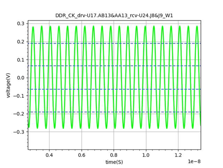
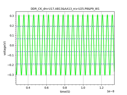
DDR_CK_T/C_A/B signal sample
Address/CMD Signal Analysis
Address/Command IO Buffer Configuration
Signals | Action | CPU | LPDDR4 DRAM |
Buffer Model | Buffer Model | ||
DDR_A[5:0] DDR_ATB[1:0] DDR_CAL | Write | lpddr4_ocd_40p_40n | CA_INPUT_ODT80_VOH30_4266 |
DDR_CS_N[4:0] DDR_CKE[1:0] | Write | lpddr4_ocd_40p_40n | CS_INPUT_ODT80_VOH30_4266 |
DDR0 – Address/Command Signal Analysis
Signal/Dram | Status | Setup | Hold | Pulse Width | |||||||||||
# | Signal | Accessed DRAM | Pass/Fail | Widest horizontal eye [mV] | Reference voltage used [mV] | Measurement [ps] | Base Requirement [ps] | Margin [ps] | Measurement [ps] | Base Requirement [ps] | Margin [ps] | Measurement [ps] | Base Requirement [ps] | Margin [ps] | Monotonic |
1 | DDR_A_0_ | U24.H2 | Fail | 161.2 | 254.8 | Fail | -93.6 | Fail | Fail | -93.6 | Fail | Fail | Fail | Fail | Pass |
2 | DDR_A_0_ | U24.R2 | Fail | 161.5 | 254.8 | Fail | -93.6 | Fail | Fail | -93.6 | Fail | Fail | Fail | Fail | Pass |
3 | DDR_A_0_ | U25.H2 | Fail | 160.7 | 254.9 | Fail | -93.6 | Fail | Fail | -93.6 | Fail | Fail | Fail | Fail | Pass |
4 | DDR_A_0_ | U25.R2 | Fail | 160.4 | 254.9 | Fail | -93.6 | Fail | Fail | -93.6 | Fail | Fail | Fail | Fail | Pass |
5 | DDR_A_1_ | U24.J2 | Fail | 163.3 | 254.8 | 49.6 | -93.6 | -52 | 49.3 | -93.6 | -52.3 | 395.7 | -374.5 | 5.2 | Pass |
6 | DDR_A_1_ | U24.P2 | Fail | 163.3 | 254.8 | 50 | -93.6 | -51.6 | 50.3 | -93.6 | -51.3 | 395.3 | -374.5 | 4.8 | Pass |
7 | DDR_A_1_ | U25.J2 | Fail | 158.7 | 254.9 | 73.7 | -93.6 | -27.9 | 48.2 | -93.6 | -53.4 | 403.9 | -374.5 | 13.4 | Pass |
8 | DDR_A_1_ | U25.P2 | Fail | 158.6 | 254.9 | 74.4 | -93.6 | -27.2 | 48.8 | -93.6 | -52.8 | 402.5 | -374.5 | 12 | Pass |
9 | DDR_A_2_ | U24.H9 | Fail | 160.1 | 254.8 | 57 | -93.6 | -44.6 | 70.3 | -93.6 | -31.3 | 405.6 | -374.5 | 15.1 | Pass |
10 | DDR_A_2_ | U24.R9 | Fail | 159.4 | 254.8 | 61.6 | -93.6 | -40 | 73 | -93.6 | -28.6 | 403.5 | -374.5 | 13 | Pass |
11 | DDR_A_2_ | U25.H9 | Fail | 159.2 | 254.9 | 33.3 | -93.6 | -68.3 | 34 | -93.6 | -67.6 | 405.2 | -374.5 | 14.7 | Pass |
12 | DDR_A_2_ | U25.R9 | Fail | 158.6 | 254.9 | 37.9 | -93.6 | -63.7 | 28.2 | -93.6 | -73.4 | 404.5 | -374.5 | 14 | Pass |
13 | DDR_A_3_ | U24.H10 | Fail | 161 | 254.8 | 53.1 | -93.6 | -48.5 | 55.5 | -93.6 | -46.1 | 399.1 | -374.5 | 8.6 | Pass |
14 | DDR_A_3_ | U24.R10 | Fail | 161.2 | 254.8 | 60.3 | -93.6 | -41.3 | 57.4 | -93.6 | -44.2 | 397.5 | -374.5 | 7 | Pass |
DDR0 – Address/Command Signal Analysis
Signal/Dram | Status | Setup | Hold | Pulse Width | |||||||||||
# | Signal | Accessed DRAM | Pass/Fail | Widest horizontal eye [mV] | Reference voltage used [mV] | Measurement [ps] | Base Requirement [ps] | Margin [ps] | Measurement [ps] | Base Requirement [ps] | Margin [ps] | Measurement [ps] | Base Requirement [ps] | Margin [ps] | Monotonic |
15 | DDR_A_3_ | U25.H10 | Fail | 159.6 | 254.9 | 16.7 | -93.6 | -84.9 | 9.6 | -93.6 | -92 | 405.4 | -374.5 | 14.9 | Pass |
16 | DDR_A_3_ | U25.R10 | Fail | 159.3 | 254.9 | 25.4 | -93.6 | -76.2 | 15.6 | -93.6 | -86 | 405.1 | -374.5 | 14.6 | Pass |
17 | DDR_A_4_ | U24.H11 | Fail | 155 | 254.8 | 66.2 | -93.6 | -35.4 | 52 | -93.6 | -49.6 | 415.7 | -374.5 | 25.2 | Pass |
18 | DDR_A_4_ | U24.R11 | Fail | 156.4 | 254.8 | 68 | -93.6 | -33.6 | 50 | -93.6 | -51.6 | 412.7 | -374.5 | 22.2 | Pass |
19 | DDR_A_4_ | U25.H11 | Fail | 156.1 | 254.9 | 45.3 | -93.6 | -56.3 | 44.6 | -93.6 | -57 | 402.2 | -374.5 | 11.7 | Pass |
20 | DDR_A_4_ | U25.R11 | Fail | 156.1 | 254.9 | 44 | -93.6 | -57.6 | 44.2 | -93.6 | -57.4 | 404 | -374.5 | 13.5 | Pass |
21 | DDR_A_5_ | U24.J11 | Fail | 160.6 | 254.8 | 40.4 | -93.6 | -61.2 | 43.8 | -93.6 | -57.8 | 405.4 | -374.5 | 14.9 | Pass |
22 | DDR_A_5_ | U24.P11 | Fail | 160.8 | 254.8 | 40.8 | -93.6 | -60.8 | 41.7 | -93.6 | -59.9 | 403.5 | -374.5 | 13 | Pass |
23 | DDR_A_5_ | U25.J11 | Fail | 162.2 | 254.9 | Fail | -93.6 | Fail | Fail | -93.6 | Fail | Fail | Fail | Fail | Pass |
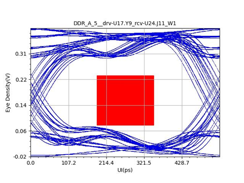
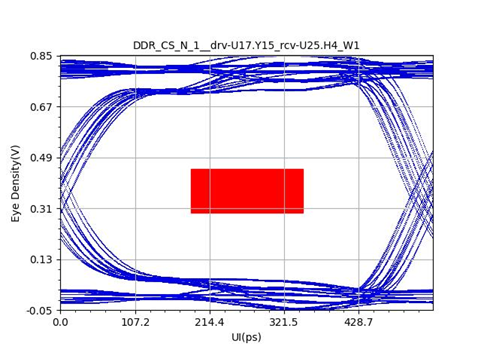
Address/Command signal sample
DQ/DM/DQS Signal Analysis – Write
DQ/DQS IO Buffer Configuration – Write
Signals | Action | CPU | LPDDR4 DRAM | ||
ODT | Buffer Model | ODT | Buffer Model | ||
DDR_DQS[3:0] DDR_DQS_N[3:0] | Write | OFF | lpddr4_ocd_40p_40n_diff | 40 | DQS_IN_ODT40_VOH30_4266 |
DDR_DQ[31:0] DDR_DM[3:0] | Write | OFF | lpddr4_ocd_40p_40n | 40 | DQ_IN_ODT40_VOH30_4266 |
DDR0-DQ/DQS/DM Signal Analysis- Write
Signal/Controller/DRAM | Status | Setup | Hold | Pulse Width | ||||||||||||
# | Signal | Driving Controller.Pin | Receiving DRAM.Pin | Pass/Fail | Widest horizontal eye [mV] | Reference voltage used [mV] | Measurement [ps] | Base Requirement [ps] | Margin [ps] | Measurement [ps] | Base Requirement [ps] | Margin [ps] | Measurement [ps] | Base Requirement [ps] | Margin [ps] | Monotonic |
1 | DDR_DQ_0_ | U17.W20 | U24.B2 | Pass | 159 | 149.9 | 82.1 | -33.4 | 40.7 | 82 | -33.4 | 40.6 | 248.5 | -120.4 | 112.1 | Pass |
2 | DDR_DQ_0_ | U17.W20 | U25.B2 | Pass | 148 | 148.1 | 86.8 | -33.4 | 45.4 | 85.9 | -33.4 | 44.5 | 247.3 | -120.4 | 110.9 | Pass |
3 | DDR_DQ_1_ | U17.W21 | U24.C2 | Pass | 151.2 | 149.9 | 85.9 | -33.4 | 44.5 | 85.5 | -33.4 | 44.1 | 252.4 | -120.4 | 116.1 | Pass |
4 | DDR_DQ_1_ | U17.W21 | U25.C2 | Pass | 153.2 | 148.1 | 88.1 | -33.4 | 46.7 | 87.4 | -33.4 | 46 | 250.3 | -120.4 | 113.9 | Pass |
5 | DDR_DQ_2_ | U17.W19 | U24.E2 | Pass | 155.4 | 149.9 | 80.7 | -33.4 | 39.3 | 81.2 | -33.4 | 39.8 | 246.8 | -120.4 | 110.4 | Pass |
6 | DDR_DQ_2_ | U17.W19 | U25.E2 | Pass | 147.4 | 148.1 | 85.9 | -33.4 | 44.5 | 85.8 | -33.4 | 44.4 | 250.2 | -120.4 | 113.9 | Pass |
7 | DDR_DQ_3_ | U17.W18 | U24.F2 | Pass | 155.9 | 149.9 | 80.6 | -33.4 | 39.2 | 80.5 | -33.4 | 39.1 | 245 | -120.4 | 108.6 | Pass |
8 | DDR_DQ_3_ | U17.W18 | U25.F2 | Pass | 153.8 | 148.1 | 84.8 | -33.4 | 43.4 | 84.9 | -33.4 | 43.5 | 248.3 | -120.4 | 111.9 | Pass |
9 | DDR_DQ_4_ | U17.W17 | U24.F4 | Pass | 149.2 | 149.9 | 81.6 | -33.4 | 40.2 | 82.2 | -33.4 | 40.8 | 245.3 | -120.4 | 109 | Pass |
10 | DDR_DQ_4_ | U17.W17 | U25.F4 | Pass | 144.3 | 148.1 | 86.4 | -33.4 | 45 | 87.1 | -33.4 | 45.7 | 247.3 | -120.4 | 110.9 | Pass |
11 | DDR_DQ_5_ | U17.V15 | U24.E4 | Pass | 151.7 | 149.9 | 83.8 | -33.4 | 42.4 | 83.7 | -33.4 | 42.3 | 251.7 | -120.4 | 115.3 | Pass |
12 | DDR_DQ_5_ | U17.V15 | U25.E4 | Pass | 148 | 148.1 | 88.3 | -33.4 | 46.9 | 87.9 | -33.4 | 46.5 | 251.5 | -120.4 | 115.1 | Pass |
13 | DDR_DQ_6_ | U17.AA21 | U24.C4 | Pass | 152.1 | 149.9 | 81.5 | -33.4 | 40.1 | 82.1 | -33.4 | 40.7 | 247.1 | -120.4 | 110.7 | Pass |
14 | DDR_DQ_6_ | U17.AA21 | U25.C4 | Pass | 150.1 | 148.1 | 83.4 | -33.4 | 42 | 83.2 | -33.4 | 41.8 | 244.3 | -120.4 | 108 | Pass |
15 | DDR_DQ_7_ | U17.Y19 | U24.B4 | Pass | 154.9 | 149.9 | 82.1 | -33.4 | 40.7 | 81.8 | -33.4 | 40.4 | 248.4 | -120.4 | 112 | Pass |
16 | DDR_DQ_7_ | U17.Y19 | U25.B4 | Pass | 154 | 148.1 | 84.8 | -33.4 | 43.4 | 85.3 | -33.4 | 43.9 | 245.8 | -120.4 | 109.4 | Pass |
17 | DDR_DQ_8_ | U17.V14 | U24.B11 | Pass | 153.8 | 149.9 | 95 | -33.4 | 53.6 | 94.1 | -33.4 | 52.7 | 259.1 | -120.4 | 122.7 | Pass |
18 | DDR_DQ_8_ | U17.V14 | U25.B11 | Pass | 153.7 | 148.1 | 94.2 | -33.4 | 52.8 | 95.2 | -33.4 | 53.8 | 260 | -120.4 | 123.6 | Pass |
19 | DDR_DQ_9_ | U17.Y17 | U24.C11 | Pass | 144.5 | 149.9 | 96.3 | -33.4 | 54.9 | 95.7 | -33.4 | 54.3 | 255.8 | -120.4 | 119.4 | Pass |
20 | DDR_DQ_9_ | U17.Y17 | U25.C11 | Pass | 146.2 | 148.1 | 94.5 | -33.4 | 53.1 | 94 | -33.4 | 52.6 | 254.4 | -120.4 | 118.1 | Pass |
21 | DDR_DQ_10_ | U17.W16 | U24.E11 | Pass | 143 | 149.9 | 94.2 | -33.4 | 52.8 | 94.5 | -33.4 | 53.1 |
22 | DDR_DQ_10_ | U17.W16 | U25.E11 | Pass | 143.8 | 148.1 | 92.6 | -33.4 | 51.2 | 91.6 | -33.4 | 50.2 |
23 | DDR_DQ_11_ | U17.Y18 | U24.F11 | Pass | 144.7 | 149.9 | 95.2 | -33.4 | 53.8 | 95.4 | -33.4 | 54 |
24 | DDR_DQ_11_ | U17.Y18 | U25.F11 | Pass | 146.2 | 148.1 | 93.2 | -33.4 | 51.8 | 92.8 | -33.4 | 51.4 |
25 | DDR_DQ_12_ | U17.AB19 | U24.F9 | Pass | 143.5 | 149.9 | 92.4 | -33.4 | 51 | 92.1 | -33.4 | 50.7 |
26 | DDR_DQ_12_ | U17.AB19 | U25.F9 | Pass | 145 | 148.1 | 91.7 | -33.4 | 50.3 | 91.2 | -33.4 | 49.8 |
27 | DDR_DQ_13_ | U17.W14 | U24.E9 | Pass | 144.7 | 149.9 | 93.8 | -33.4 | 52.4 | 94.7 | -33.4 | 53.3 |
28 | DDR_DQ_13_ | U17.W14 | U25.E9 | Pass | 145.9 | 148.1 | 94 | -33.4 | 52.6 | 93.6 | -33.4 | 52.2 |
29 | DDR_DQ_14_ | U17.AA17 | U24.C9 | Pass | 144.9 | 149.9 | 95.4 | -33.4 | 54 | 94.8 | -33.4 | 53.4 |
30 | DDR_DQ_14_ | U17.AA17 | U25.C9 | Pass | 144.7 | 148.1 | 93.9 | -33.4 | 52.5 | 94.6 | -33.4 | 53.2 |
31 | DDR_DQ_15_ | U17.AB18 | U24.B9 | Pass | 144.4 | 149.9 | 93.2 | -33.4 | 51.8 | 94.1 | -33.4 | 52.7 |
32 | DDR_DQ_15_ | U17.AB18 | U25.B9 | Pass | 144.9 | 148.1 | 92.8 | -33.4 | 51.4 | 93.1 | -33.4 | 51.7 |
33 | DDR_DQ_16_ | U17.AB6 | U24.AA2 | Pass | 153.2 | 149.9 | 82.2 | -33.4 | 40.8 | 82.4 | -33.4 | 41 |
34 | DDR_DQ_16_ | U17.AB6 | U25.AA2 | Pass | 147.6 | 148.1 | 86.7 | -33.4 | 45.3 | 86.2 | -33.4 | 44.8 |
35 | DDR_DQ_17_ | U17.Y7 | U24.Y2 | Pass | 152 | 149.9 | 82.8 | -33.4 | 41.4 | 82.7 | -33.4 | 41.3 |
36 | DDR_DQ_17_ | U17.Y7 | U25.Y2 | Pass | 145.1 | 148.1 | 92.7 | -33.4 | 51.3 | 92.4 | -33.4 | 51 |
DDR0-DQ/DQS/DM Signal Analysis- Write
Signal/Controller/DRAM | Status | Setup | Hold | Pulse Width | ||||||||||||
# | Signal | Driving Controller.Pin | Receiving DRAM.Pin | Pass/Fail | Widest horizontal eye [mV] | Reference voltage used [mV] | Measurement [ps] | Base Requirement [ps] | Margin [ps] | Measurement [ps] | Base Requirement [ps] | Margin [ps] | Measurement [ps] | Base Requirement [ps] | Margin [ps] | Monotonic |
37 | DDR_DQ_18_ | U17.AB5 | U24.V2 | Pass | 151.3 | 149.9 | 81.4 | -33.4 | 40 | 81.2 | -33.4 | 39.8 | 246 | -120.4 | 109.6 | Pass |
38 | DDR_DQ_18_ | U17.AB5 | U25.V2 | Pass | 145.7 | 148.1 | 90.5 | -33.4 | 49.1 | 89.7 | -33.4 | 48.3 | 249.8 | -120.4 | 113.5 | Pass |
39 | DDR_DQ_19_ | U17.AB3 | U24.U2 | Pass | 155 | 149.9 | 79.4 | -33.4 | 38 | 79.8 | -33.4 | 38.4 | 252 | -120.4 | 115.6 | Pass |
40 | DDR_DQ_19_ | U17.AB3 | U25.U2 | Pass | 148.2 | 148.1 | 93.5 | -33.4 | 52.1 | 92.8 | -33.4 | 51.4 | 257.2 | -120.4 | 120.8 | Pass |
41 | DDR_DQ_20_ | U17.AB2 | U24.U4 | Pass | 156.6 | 149.9 | 81.6 | -33.4 | 40.2 | 81.3 | -33.4 | 39.9 | 257.6 | -120.4 | 121.2 | Pass |
42 | DDR_DQ_20_ | U17.AB2 | U25.U4 | Pass | 152.2 | 148.1 | 91.2 | -33.4 | 49.8 | 91.7 | -33.4 | 50.3 | 259.2 | -120.4 | 122.9 | Pass |
43 | DDR_DQ_21_ | U17.V9 | U24.V4 | Pass | 149.5 | 149.9 | 86 | -33.4 | 44.6 | 86.3 | -33.4 | 44.9 | 252.2 | -120.4 | 115.8 | Pass |
44 | DDR_DQ_21_ | U17.V9 | U25.V4 | Pass | 143.7 | 148.1 | 93.4 | -33.4 | 52 | 92.6 | -33.4 | 51.2 | 252.1 | -120.4 | 115.7 | Pass |
45 | DDR_DQ_22_ | U17.Y6 | U24.Y4 | Pass | 148.8 | 149.9 | 86.1 | -33.4 | 44.7 | 85.3 | -33.4 | 43.9 | 249.4 | -120.4 | 113 | Pass |
46 | DDR_DQ_22_ | U17.Y6 | U25.Y4 | Pass | 144 | 148.1 | 92.2 | -33.4 | 50.8 | 93.1 | -33.4 | 51.7 | 249.5 | -120.4 | 113.1 | Pass |
47 | DDR_DQ_23_ | U17.W7 | U24.AA4 | Pass | 155.5 | 149.9 | 83.1 | -33.4 | 41.7 | 83.5 | -33.4 | 42.1 | 251.8 | -120.4 | 115.4 | Pass |
48 | DDR_DQ_23_ | U17.W7 | U25.AA4 | Pass | 152.7 | 148.1 | 90.6 | -33.4 | 49.2 | 91.3 | -33.4 | 49.9 | 253.1 | -120.4 | 116.8 | Pass |
49 | DDR_DQ_24_ | U17.Y4 | U24.AA11 | Pass | 140.8 | 149.9 | 89.5 | -33.4 | 48.1 | 89.6 | -33.4 | 48.2 | 253.4 | -120.4 | 117 | Pass |
50 | DDR_DQ_24_ | U17.Y4 | U25.AA11 | Pass | 142.2 | 148.1 | 92.9 | -33.4 | 51.5 | 91.9 | -33.4 | 50.5 | 254.7 | -120.4 | 118.3 | Pass |
51 | DDR_DQ_25_ | U17.AA3 | U24.Y11 | Pass | 145.6 | 149.9 | 89 | -33.4 | 47.6 | 88.1 | -33.4 | 46.7 | 254.3 | -120.4 | 117.9 | Pass |
52 | DDR_DQ_25_ | U17.AA3 | U25.Y11 | Pass | 141 | 148.1 | 89.9 | -33.4 | 48.5 | 89.7 | -33.4 | 48.3 | 251.3 | -120.4 | 114.9 | Pass |
53 | DDR_DQ_26_ | U17.AA1 | U24.V11 | Pass | 144.2 | 149.9 | 90.4 | -33.4 | 49 | 91.2 | -33.4 | 49.8 | 259.9 | -120.4 | 123.5 | Pass |
54 | DDR_DQ_26_ | U17.AA1 | U25.V11 | Pass | 141.2 | 148.1 | 92.1 | -33.4 | 50.7 | 91.6 | -33.4 | 50.2 | 259.1 | -120.4 | 122.7 | Pass |
55 | DDR_DQ_27_ | U17.V8 | U24.U11 | Pass | 144.6 | 149.9 | 87.9 | -33.4 | 46.5 | 88.7 | -33.4 | 47.3 | 256.3 | -120.4 | 119.9 | Pass |
56 | DDR_DQ_27_ | U17.V8 | U25.U11 | Pass | 140.4 | 148.1 | 90.6 | -33.4 | 49.2 | 89.9 | -33.4 | 48.5 | 253.8 | -120.4 | 117.5 | Pass |
57 | DDR_DQ_28_ | U17.W5 | U24.U9 | Pass | 142.6 | 149.9 | 88.8 | -33.4 | 47.4 | 89.9 | -33.4 | 48.5 | 255.9 |
58 | DDR_DQ_28_ | U17.W5 | U25.U9 | Pass | 145.4 | 148.1 | 89.5 | -33.4 | 48.1 | 89.1 | -33.4 | 47.7 | 254.3 |
59 | DDR_DQ_29_ | U17.W6 | U24.V9 | Pass | 147 | 149.9 | 90.2 | -33.4 | 48.8 | 89.7 | -33.4 | 48.3 | 254.7 |
60 | DDR_DQ_29_ | U17.W6 | U25.V9 | Pass | 155.8 | 148.1 | 91.1 | -33.4 | 49.7 | 90.7 | -33.4 | 49.3 | 255.8 |
61 | DDR_DQ_30_ | U17.W3 | U24.Y9 | Pass | 143.3 | 149.9 | 89.4 | -33.4 | 48 | 89.1 | -33.4 | 47.7 | 255.4 |
62 | DDR_DQ_30_ | U17.W3 | U25.Y9 | Pass | 141.2 | 148.1 | 89.9 | -33.4 | 48.5 | 90.2 | -33.4 | 48.8 | 257.2 |
63 | DDR_DQ_31_ | U17.W4 | U24.AA9 | Pass | 143.6 | 149.9 | 88.6 | -33.4 | 47.2 | 88.3 | -33.4 | 46.9 | 252.1 |
64 | DDR_DQ_31_ | U17.W4 | U25.AA9 | Pass | 142 | 148.1 | 90.2 | -33.4 | 48.8 | 90.7 | -33.4 | 49.3 | 253.8 |
65 | DDR_DM_0_ | U17.Y20 | U24.C3 | Pass | 152.1 | 149.9 | 83.7 | -33.4 | 42.3 | 84.3 | -33.4 | 42.9 | 247.7 |
66 | DDR_DM_0_ | U17.Y20 | U25.C3 | Pass | 149.8 | 148.1 | 87.3 | -33.4 | 45.9 | 86.7 | -33.4 | 45.3 | 247.2 |
67 | DDR_DM_1_ | U17.AA19 | U24.C10 | Pass | 143.7 | 149.9 | 93.4 | -33.4 | 52 | 93.1 | -33.4 | 51.7 | 251 |
68 | DDR_DM_1_ | U17.AA19 | U25.C10 | Pass | 145.7 | 148.1 | 92.1 | -33.4 | 50.7 | 92.9 | -33.4 | 51.5 | 250.7 |
69 | DDR_DM_2_ | U17.AB4 | U24.Y3 | Pass | 153.2 | 149.9 | 81.3 | -33.4 | 39.9 | 81.9 | -33.4 | 40.5 | 248.4 |
70 | DDR_DM_2_ | U17.AB4 | U25.Y3 | Pass | 148.2 | 148.1 | 90.3 | -33.4 | 48.9 | 90.5 | -33.4 | 49.1 | 249.8 |
71 | DDR_DM_3_ | U17.Y1 | U24.Y10 | Pass | 155.6 | 149.9 | 87.5 | -33.4 | 46.1 | 88.5 | -33.4 | 47.1 | 255.2 |
72 | DDR_DM_3_ | U17.Y1 | U25.Y10 | Pass | 141.7 | 148.1 | 86.7 | -33.4 | 45.3 | 86.9 | -33.4 | 45.5 | 254.6 |
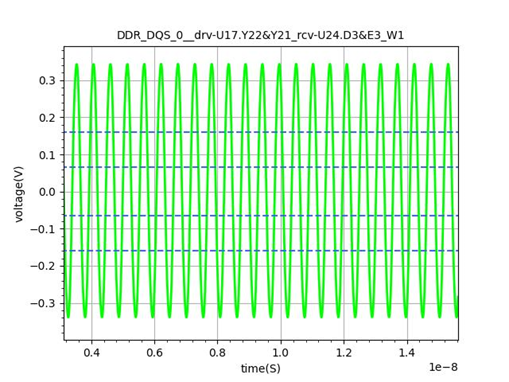
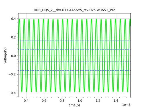
DQS Sample – Write
DQ/DQS/DM Eye Sample – Write
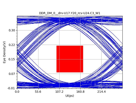
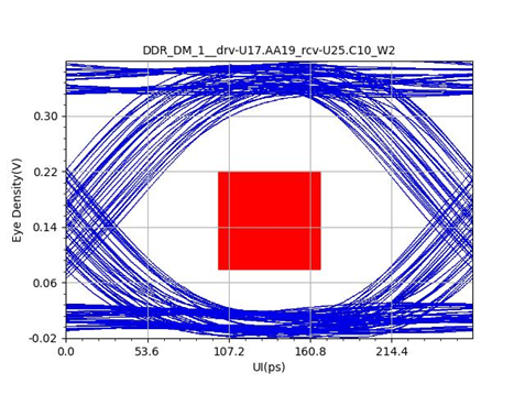
DQ/DQS/DM Eye Sample – Write
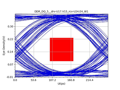

DQ/DQS/DM Eye Sample – Write
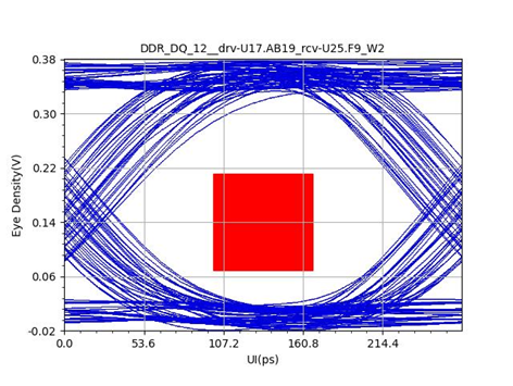
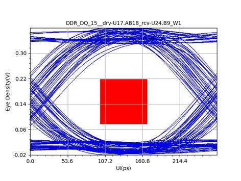

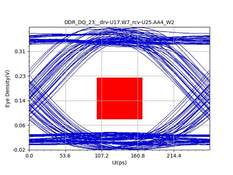
DQ/DQS/DM Eye Sample – Write
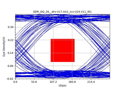
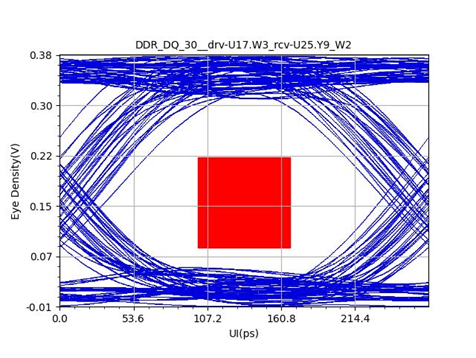
DQ/DM/DQS Signal Analysis – Read
DQ/DQS IO Buffer Configuration – Read
Signals | Action | CPU | LPDDR4 DRAM | ||
ODT | Buffer Model | ODT | Buffer Model | ||
DDR_DQS[3:0] DDR_DQS_N[3:0] | Read | 40 | lpddr4_odt_40_diff | OFF | DQS_PD40_ODT40_VOH30_4266 |
DDR_DQ[31:0] DDR_DM[3:0] | Read | 40 | lpddr4_odt_40 | OFF | DQ_PD40_ODT40_VOH30_4266 |
DQ/DQS/DM Signal Analysis- Read
Signal/DRAM/Controller | Status | Setup | Hold | Pulse Width | |||||||||||
# | Signal | Driving DRAM.Pin | Receiving Controller.Pin | Pass/Fail | Widest Horizontal Eye [mV] | Reference Voltage Used [mV] | Measurement [ps] | Base Requirement [ps] | Margin [ps] | Measurement [ps] | Base Requirement [ps] | Margin [ps] | Measurement [ps] | ||
1 | DDR_DQ_0_ | U24.B2 | U17.W20 | Fail | 271.9 | 178.4 | Fail | -26.7 | Fail | Fail | -26.7 | Fail | Fail | Fail | Fail |
2 | DDR_DQ_0_ | U25.B2 | U17.W20 | Fail | 274.5 | 179.9 | Fail | -26.7 | Fail | Fail | -26.7 | Fail | Fail | Fail | Fail |
3 | DDR_DQ_1_ | U24.C2 | U17.W21 | Fail | 266.8 | 178.4 | Fail | -26.7 | Fail | Fail | -26.7 | Fail | Fail | Fail | Fail |
4 | DDR_DQ_1_ | U25.C2 | U17.W21 | Fail | 215.2 | 179.9 | Fail | -26.7 | Fail | Fail | -26.7 | Fail | Fail | Fail | Fail |
5 | DDR_DQ_2_ | U24.E2 | U17.W19 | Fail | 80.9 | 178.4 | Fail | -26.7 | Fail | Fail | -26.7 | Fail | Fail | Fail | Fail |
6 | DDR_DQ_2_ | U25.E2 | U17.W19 | Fail | 77.4 | 179.9 | Fail | -26.7 | Fail | Fail | -26.7 | Fail | Fail | Fail | Fail |
7 | DDR_DQ_3_ | U24.F2 | U17.W18 | Fail | 271.5 | 178.4 | Fail | -26.7 | Fail | Fail | -26.7 | Fail | Fail | Fail | Fail |
8 | DDR_DQ_3_ | U25.F2 | U17.W18 | Fail | 212.4 | 179.9 | Fail | -26.7 | Fail | Fail | -26.7 | Fail | Fail | Fail | Fail |
9 | DDR_DQ_4_ | U24.F4 | U17.W17 | Fail | 282.8 | 178.4 | Fail | -26.7 | Fail | Fail | -26.7 | Fail | Fail | Fail | Fail |
10 | DDR_DQ_4_ | U25.F4 | U17.W17 | Fail | 260.8 | 179.9 | Fail | -26.7 | Fail | Fail | -26.7 | Fail | Fail | Fail | Fail |
11 | DDR_DQ_5_ | U24.E4 | U17.V15 | Fail | 176.1 | 178.4 | Fail | -26.7 | Fail | Fail | -26.7 | Fail | Fail | Fail | Fail |
12 | DDR_DQ_5_ | U25.E4 | U17.V15 | Fail | 177 | 179.9 | Fail | -26.7 | Fail | Fail | -26.7 | Fail | Fail | Fail | Fail |
13 | DDR_DQ_6_ | U24.C4 | U17.AA21 | Fail | 270.4 | 178.4 | Fail | -26.7 | Fail | Fail | -26.7 | Fail | Fail | Fail | Fail |
14 | DDR_DQ_6_ | U25.C4 | U17.AA21 | Fail | 279.9 | 179.9 | Fail | -26.7 | Fail | Fail | -26.7 | Fail | Fail | Fail | Fail |
15 | DDR_DQ_7_ | U24.B4 | U17.Y19 | Fail | 267.4 | 178.4 | Fail | -26.7 | Fail | Fail | -26.7 | Fail | Fail | Fail | Fail |
16 | DDR_DQ_7_ | U25.B4 | U17.Y19 | Fail | 271.5 | 179.9 | Fail | -26.7 | Fail | Fail | -26.7 | Fail | Fail | Fail | Fail |
17 | DDR_DQ_8_ | U24.B11 | U17.V14 | Fail | 241.7 | 178.4 | Fail | -26.7 | Fail | Fail | -26.7 | Fail | Fail | Fail | Fail |
18 | DDR_DQ_8_ | U25.B11 | U17.V14 | Fail | 241.6 | 179.9 | Fail | -26.7 | Fail | Fail | -26.7 | Fail | Fail |
19 | DDR_DQ_9_ | U24.C11 | U17.Y17 | Fail | 280.7 | 178.4 | Fail | -26.7 | Fail | Fail | -26.7 | Fail | Fail |
20 | DDR_DQ_9_ | U25.C11 | U17.Y17 | Fail | 278.6 | 179.9 | Fail | -26.7 | Fail | Fail | -26.7 | Fail | Fail |
21 | DDR_DQ_10_ | U24.E11 | U17.W16 | Fail | 274.1 | 178.4 | Fail | -26.7 | Fail | Fail | -26.7 | Fail | Fail |
22 | DDR_DQ_10_ | U25.E11 | U17.W16 | Fail | 73.1 | 179.9 | Fail | -26.7 | Fail | Fail | -26.7 | Fail | Fail |
23 | DDR_DQ_11_ | U24.F11 | U17.Y18 | Fail | 273.1 | 178.4 | Fail | -26.7 | Fail | Fail | -26.7 | Fail | Fail |
24 | DDR_DQ_11_ | U25.F11 | U17.Y18 | Fail | 269.9 | 179.9 | Fail | -26.7 | Fail | Fail | -26.7 | Fail | Fail |
25 | DDR_DQ_12_ | U24.F9 | U17.AB19 | Fail | 280 | 178.4 | Fail | -26.7 | Fail | Fail | -26.7 | Fail | Fail |
26 | DDR_DQ_12_ | U25.F9 | U17.AB19 | Fail | 279.3 | 179.9 | Fail | -26.7 | Fail | Fail | -26.7 | Fail | Fail |
27 | DDR_DQ_13_ | U24.E9 | U17.W14 | Fail | 271.6 | 178.4 | Fail | -26.7 | Fail | Fail | -26.7 | Fail | Fail |
28 | DDR_DQ_13_ | U25.E9 | U17.W14 | Fail | 270.4 | 179.9 | Fail | -26.7 | Fail | Fail | -26.7 | Fail | Fail |
29 | DDR_DQ_14_ | U24.C9 | U17.AA17 | Fail | 278.9 | 178.4 | Fail | -26.7 | Fail | Fail | -26.7 | Fail | Fail |
30 | DDR_DQ_14_ | U25.C9 | U17.AA17 | Fail | 278.8 | 179.9 | Fail | -26.7 | Fail | Fail | -26.7 | Fail | Fail |
31 | DDR_DQ_15_ | U24.B9 | U17.AB18 | Fail | 265.9 | 178.4 | Fail | -26.7 | Fail | Fail | -26.7 | Fail | Fail |
32 | DDR_DQ_15_ | U25.B9 | U17.AB18 | Fail | 265.6 | 179.9 | Fail | -26.7 | Fail | Fail | -26.7 | Fail | Fail |
DQ/DQS/DM Signal Analysis- Read
Signal/DRAM/Controller | Status | Setup | Hold | Pulse Width | |||||||||||
# | Signal | Driving DRAM.Pin | Receiving Controller.Pin | Pass/Fail | Widest Horizontal Eye [mV] | Reference Voltage Used [mV] | Measurement [ps] | Base Requirement [ps] | Margin [ps] | Measurement [ps] | Base Requirement [ps] | Margin [ps] | Measurement [ps] | ||
33 | DDR_DQ_16_ | U24.AA2 | U17.AB6 | Fail | 82 | 178.4 | Fail | -26.7 | Fail | Fail | -26.7 | Fail | Fail | Fail | Fail |
34 | DDR_DQ_16_ | U25.AA2 | U17.AB6 | Fail | 281.6 | 179.9 | Fail | -26.7 | Fail | Fail | -26.7 | Fail | Fail | Fail | Fail |
35 | DDR_DQ_17_ | U24.Y2 | U17.Y7 | Fail | 74 | 178.4 | Fail | -26.7 | Fail | Fail | -26.7 | Fail | Fail | Fail | Fail |
36 | DDR_DQ_17_ | U25.Y2 | U17.Y7 | Fail | 76.4 | 179.9 | Fail | -26.7 | Fail | Fail | -26.7 | Fail | Fail | Fail | Fail |
37 | DDR_DQ_18_ | U24.V2 | U17.AB5 | Fail | 268.3 | 178.4 | Fail | -26.7 | Fail | Fail | -26.7 | Fail | Fail | Fail | Fail |
38 | DDR_DQ_18_ | U25.V2 | U17.AB5 | Fail | 273.3 | 179.9 | Fail | -26.7 | Fail | Fail | -26.7 | Fail | Fail | Fail | Fail |
39 | DDR_DQ_19_ | U24.U2 | U17.AB3 | Fail | 274.6 | 178.4 | Fail | -26.7 | Fail | Fail | -26.7 | Fail | Fail | Fail | Fail |
40 | DDR_DQ_19_ | U25.U2 | U17.AB3 | Fail | 286.6 | 179.9 | Fail | -26.7 | Fail | Fail | -26.7 | Fail | Fail | Fail | Fail |
41 | DDR_DQ_20_ | U24.U4 | U17.AB2 | Fail | 176.6 | 178.4 | Fail | -26.7 | Fail | Fail | -26.7 | Fail | Fail | Fail | Fail |
42 | DDR_DQ_20_ | U25.U4 | U17.AB2 | Fail | 256 | 179.9 | Fail | -26.7 | Fail | Fail | -26.7 | Fail | Fail | Fail | Fail |
43 | DDR_DQ_21_ | U24.V4 | U17.V9 | Fail | 78.2 | 178.4 | Fail | -26.7 | Fail | Fail | -26.7 | Fail | Fail | Fail | Fail |
44 | DDR_DQ_21_ | U25.V4 | U17.V9 | Fail | 79.1 | 179.9 | Fail | -26.7 | Fail | Fail | -26.7 | Fail | Fail | Fail | Fail |
45 | DDR_DQ_22_ | U24.Y4 | U17.Y6 | Fail | 280.8 | 178.4 | Fail | -26.7 | Fail | Fail | -26.7 | Fail | Fail | Fail | Fail |
46 | DDR_DQ_22_ | U25.Y4 | U17.Y6 | Fail | 280.9 | 179.9 | Fail | -26.7 | Fail | Fail | -26.7 | Fail | Fail | Fail | Fail |
47 | DDR_DQ_23_ | U24.AA4 | U17.W7 | Fail | 277.8 | 178.4 | Fail | -26.7 | Fail | Fail | -26.7 | Fail | Fail | Fail | Fail |
48 | DDR_DQ_23_ | U25.AA4 | U17.W7 | Fail | 250.3 | 179.9 | Fail | -26.7 | Fail | Fail | -26.7 | Fail | Fail | Fail | Fail |
49 | DDR_DQ_24_ | U24.AA11 | U17.Y4 | Fail | 267.3 | 178.4 | Fail | -26.7 | Fail | Fail | -26.7 | Fail | Fail | Fail | Fail |
50 | DDR_DQ_24_ | U25.AA11 | U17.Y4 | Fail | 123 | 179.9 | Fail | -26.7 | Fail | Fail | -26.7 | Fail | Fail | Fail | Fail |
51 | DDR_DQ_25_ | U24.Y11 | U17.AA3 | Fail | 144.7 | 178.4 | Fail | -26.7 | Fail | Fail | -26.7 | Fail | Fail |
52 | DDR_DQ_25_ | U25.Y11 | U17.AA3 | Fail | 199.3 | 179.9 | Fail | -26.7 | Fail | Fail | -26.7 | Fail | Fail |
53 | DDR_DQ_26_ | U24.V11 | U17.AA1 | Fail | 270 | 178.4 | Fail | -26.7 | Fail | Fail | -26.7 | Fail | Fail |
54 | DDR_DQ_26_ | U25.V11 | U17.AA1 | Fail | 271.1 | 179.9 | Fail | -26.7 | Fail | Fail | -26.7 | Fail | Fail |
55 | DDR_DQ_27_ | U24.U11 | U17.V8 | Fail | 203.2 | 178.4 | Fail | -26.7 | Fail | Fail | -26.7 | Fail | Fail |
56 | DDR_DQ_27_ | U25.U11 | U17.V8 | Fail | 77.8 | 179.9 | Fail | -26.7 | Fail | Fail | -26.7 | Fail | Fail |
57 | DDR_DQ_28_ | U24.U9 | U17.W5 | Fail | 273.7 | 178.4 | Fail | -26.7 | Fail | Fail | -26.7 | Fail | Fail |
58 | DDR_DQ_28_ | U25.U9 | U17.W5 | Fail | 101.3 | 179.9 | Fail | -26.7 | Fail | Fail | -26.7 | Fail | Fail |
59 | DDR_DQ_29_ | U24.V9 | U17.W6 | Fail | 279.5 | 178.4 | Fail | -26.7 | Fail | Fail | -26.7 | Fail | Fail |
60 | DDR_DQ_29_ | U25.V9 | U17.W6 | Fail | 207.7 | 179.9 | Fail | -26.7 | Fail | Fail | -26.7 | Fail | Fail |
61 | DDR_DQ_30_ | U24.Y9 | U17.W3 | Fail | 281.2 | 178.4 | Fail | -26.7 | Fail | Fail | -26.7 | Fail | Fail |
62 | DDR_DQ_30_ | U25.Y9 | U17.W3 | Fail | 277.8 | 179.9 | Fail | -26.7 | Fail | Fail | -26.7 | Fail | Fail |
63 | DDR_DQ_31_ | U24.AA9 | U17.W4 | Fail | 81.2 | 178.4 | Fail | -26.7 | Fail | Fail | -26.7 | Fail | Fail |
64 | DDR_DQ_31_ | U25.AA9 | U17.W4 | Fail | 80.6 | 179.9 | Fail | -26.7 | Fail | Fail | -26.7 | Fail | Fail |
DQS – Read
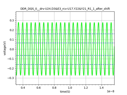
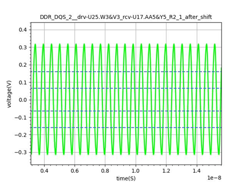
DQ Eye Sample – Read

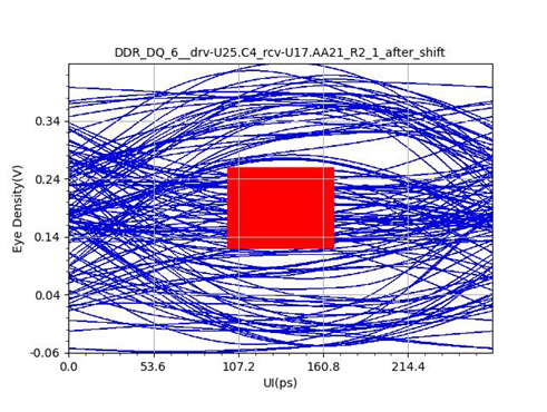
DQ Eye Sample – Read
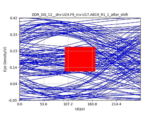

DQ Eye Sample – Read
What If Analysis
ADDR/DQ branch
The ADDR/DQ branch is very long for the structural holes limit space, which lead to big reflection and SI issue.
The LPDDR4 evaluated data rate will not exceed 1000Mbps as current design.
Another to pay attention that LPDDR4 use a completely different technology compared to DDR3/DDR4, it must be careful to design the schematics when multi SDRAMs were used
Issue