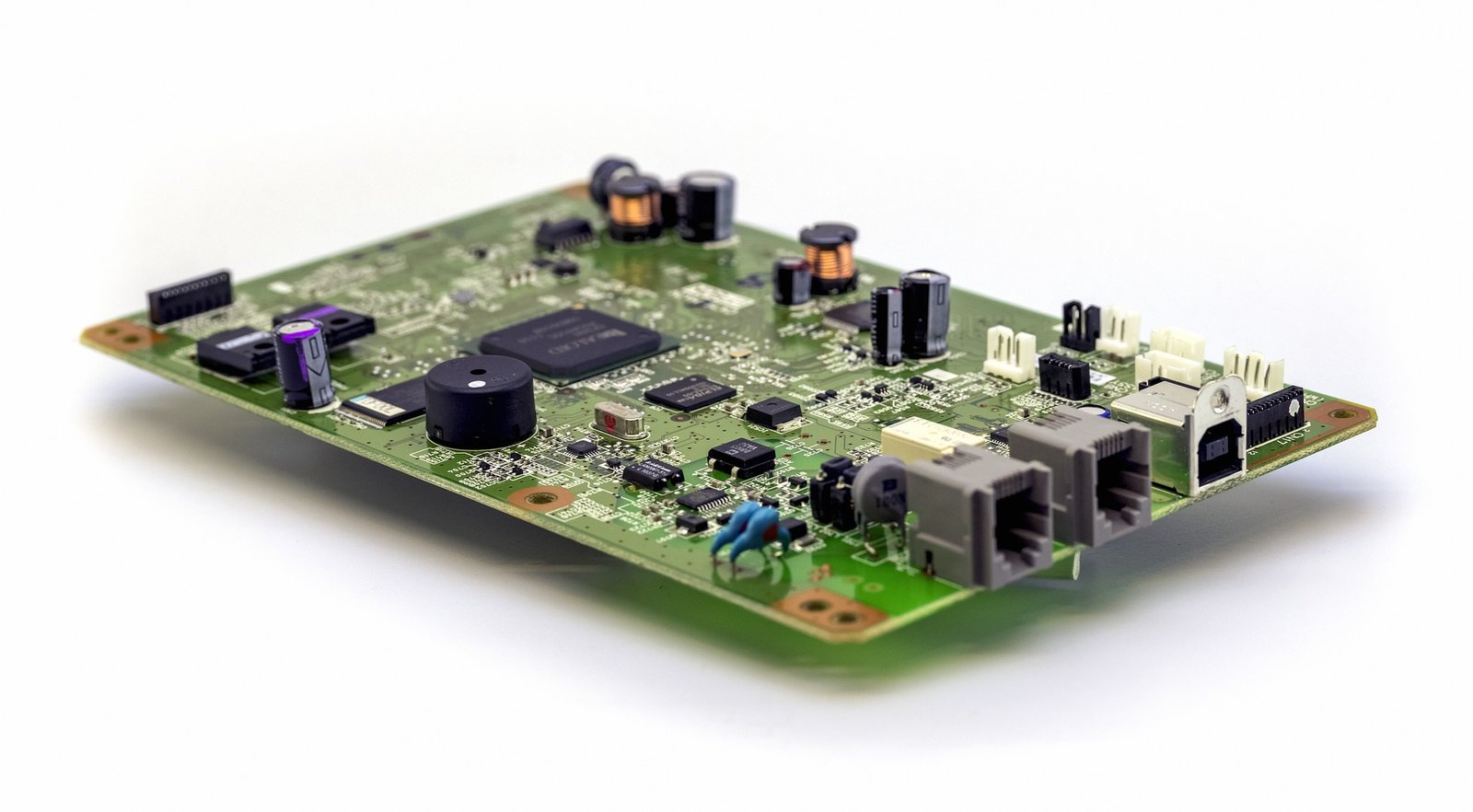
Designing a keyboard PCB (Printed Circuit Board) is a meticulous process that requires attention to detail and a strong understanding of electronic components, circuit design, and manufacturing processes. The following guide outlines the key steps in designing a custom keyboard PCB, from initial concept to ready-for-production.
1. Define Your Keyboard Layout
The first step in designing a keyboard PCB is to define the layout of your keyboard. This involves determining the number of keys, their placement, and the overall dimensions of the keyboard. Tools like Keyboard Layout Editor (KLE) can help visualize and customize layouts. During this stage, consider factors such as key spacing, ergonomic design, and any special features like media controls or backlighting.
This stage is crucial because the layout directly impacts the electrical design and the placement of components on the PCB. It’s important to finalize the layout before moving on to the schematic design, as changes at a later stage can be time-consuming and costly.
2. Schematic Design
Once the layout is set, the next step is to create the schematic. The schematic is a diagram that represents the electrical connections between the various components of the keyboard, such as switches, diodes, microcontrollers, and connectors.
Start by selecting the appropriate microcontroller based on your keyboard’s requirements. Popular choices include the ATmega32U4 or ARM Cortex-M series, depending on the complexity of your keyboard. Ensure that you include enough GPIO (General Purpose Input/Output) pins to accommodate all the keys and any additional features like RGB lighting.
Each switch on the keyboard is typically connected to the microcontroller via a matrix, reducing the number of required pins. Diodes are often placed in series with each switch to prevent ghosting (where multiple keys register when only one is pressed). The schematic should also include the necessary pull-up or pull-down resistors and capacitors for signal stability.
3. PCB Layout Design
After completing the schematic, you can begin designing the PCB layout. The layout is where the physical design of the keyboard PCB takes shape, translating the schematic into actual copper traces and component placements on the board.
In PCB design software like KiCad or Altium Designer, place the microcontroller and other major components first. Then, position the switches in alignment with the keyboard layout. The goal is to minimize the length of traces to reduce signal delay and interference. Pay careful attention to the routing of the traces, especially in the matrix, ensuring that they are clear of any obstacles and have the proper width to handle the expected current.
If your keyboard includes backlighting, you’ll need to route additional traces for the LEDs and ensure there’s enough space for resistors or other current-limiting components. For wireless keyboards, you’ll also need to consider the placement of antennas to avoid interference from other components.
4. Add Flex PCB Stiffeners
For keyboards that require a flexible PCB, such as those with curved designs or needing high durability, incorporating flex PCB stiffeners can be crucial. These stiffeners provide mechanical support and ensure the flexible sections of the PCB maintain their shape and integrity during use. They are typically added around connectors or along the edges of the board to prevent bending in critical areas.
The use of flex circuit stiffeners in keyboard PCB design is particularly important for maintaining reliability in keyboards that will undergo heavy use or are part of portable devices. Ensuring proper placement and material choice for these stiffeners can extend the life of the keyboard and improve user experience.
5. Prototyping and Testing
Once the PCB layout is complete, it’s time to move on to pcb prototyping services. Creating a prototype allows you to test the design for functionality and identify any issues before mass production. During this stage, verify that all the keys register correctly, that the microcontroller communicates as expected, and that any additional features like backlighting or wireless connectivity work properly.
Testing should also include durability checks, particularly if you’ve used pcb stiffeners or flex pcb stiffeners. This ensures that the keyboard can withstand long-term use without electrical or mechanical failure.
6. Final Adjustments and Manufacturing
After testing the prototype, make any necessary adjustments to the design. This could involve rerouting traces, adjusting the placement of components, or modifying the pcb assembly cost by optimizing the BOM (Bill of Materials). Once the design is finalized, you can prepare the files needed for production, including Gerber files, BOM, and assembly drawings.
At this stage, it is crucial to choose a reliable pcba manufacturer who can bring your design to life with precision and efficiency. Companies like ArisenTec offer turnkey pcb assembly services, providing a seamless transition from design to production. With ArisenTec’s expertise, you can ensure that your keyboard PCB is manufactured to the highest standards, with attention to detail that guarantees both performance and durability.
7. Conclusion
Designing a keyboard PCB is a complex process that requires a blend of creativity, technical expertise, and precision. By carefully planning each step, from defining the layout to finalizing the PCB design, and by incorporating key elements like flex circuit stiffeners, you can create a high-quality keyboard that meets both functional and aesthetic requirements. Partnering with an experienced manufacturer like ArisenTec ensures that your custom keyboard can go from concept to reality with efficiency and accuracy.
Choosing the Right Wires for Breadboard Wiring: A Comprehensive Guide
Breadboards are a staple in electronic circuit building, offering flexibility and ease of use for both beginners and professionals. However, one of the most critical aspects of working with breadboards is selecting the right wires. The wires you choose can impact not only the functionality of your circuit but also its longevity and ease of…
How to Improve Heat Dissipation in PCB Design
Introduction As modern electronic devices become more complex and power-dense, heat dissipation has emerged as a critical factor that directly impacts device performance and reliability. Excessive junction temperatures in electronic systems can shorten the lifespan of components and lead to system failure. Thus, optimizing the PCB (Printed Circuit Board) design to improve heat dissipation is…
Manufacturing Process of Multilayer PCBs
Multilayer PCB manufacturing methods include the plated-through hole (PTH) and high-density interconnect (HDI) methods, both achieved by combining different processes to realize the circuit board structure. Currently, the most widely used method is the PTH method, which has been developed and refined over more than half a century. The PTH method is mature in terms…


