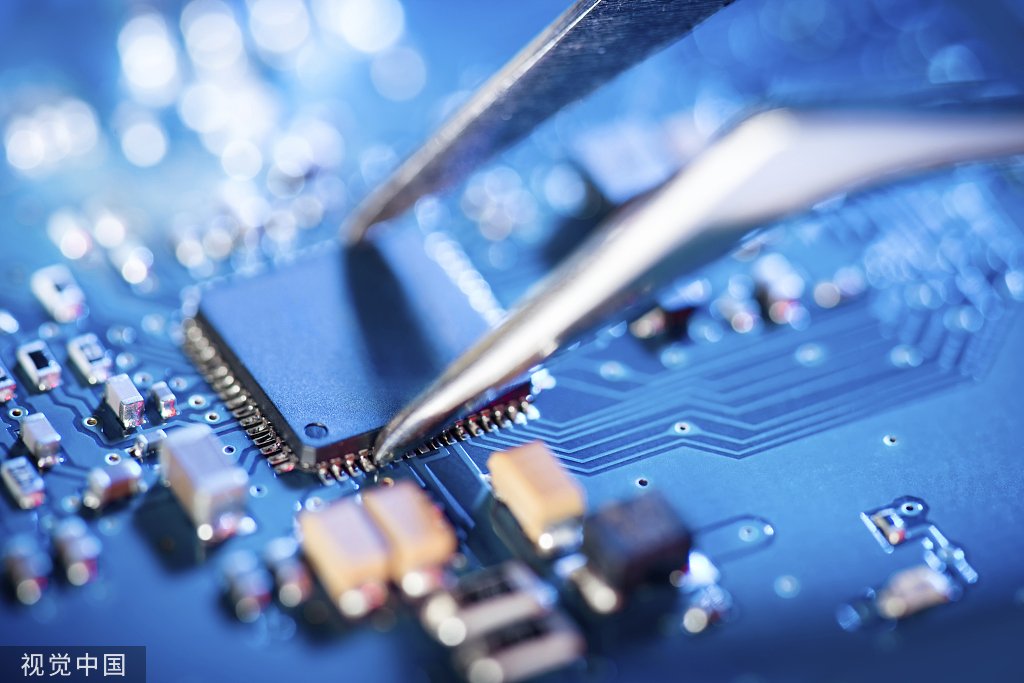
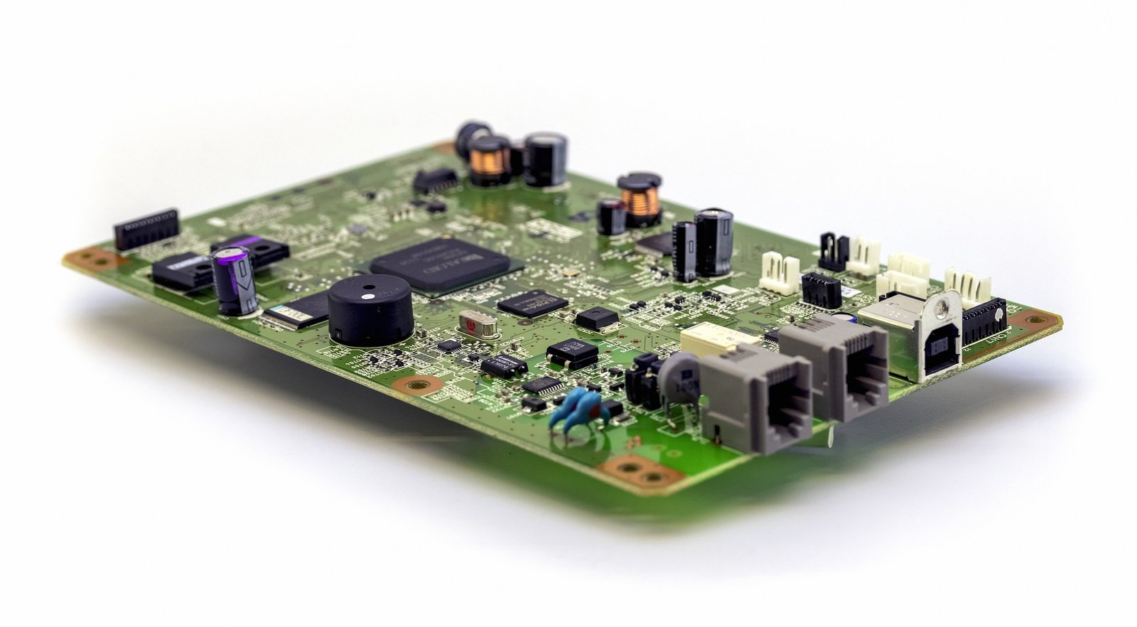
Soldering a PCB board is a fundamental skill in electronics manufacturing that requires precision and attention to detail. Proper soldering ensures reliable connections and long-lasting performance of electronic devices. Whether you are assembling a prototype or working in a pcba manufacturing environment, following the correct soldering procedure is essential for quality assurance.
1. Preparation and Safety Measures
Before beginning the soldering process, ensure that you have all necessary tools and safety equipment. This includes a soldering iron, solder wire, flux, a pair of tweezers, a desoldering pump, and safety goggles. The workspace should be clean, well-lit, and free from any flammable materials.
Proper ventilation is also crucial to avoid inhaling fumes from the solder and flux. If you are working in a pcba factory, it’s likely that these safety measures are already in place, but it’s always good practice to double-check.
2. Understanding the PCB Layout
Before soldering, it’s important to study the PCB board layout. This involves identifying all components and understanding their placement on the board. The PCB’s silk screen, which contains labels and markings, helps in correctly positioning components. Misplacing a component can lead to malfunction or even damage to the board, which is why careful examination is vital, especially when working with complex designs like flex pcb stiffener systems.
3. Component Placement
Once you are familiar with the layout, start placing components onto the PCB. Insert each component’s leads through the corresponding holes in the board. For surface-mount technology (SMT), place the components onto the pads designed for them. This step requires steady hands and precise alignment, particularly when dealing with small components or complex assemblies like those seen in turnkey pcb assembly.
4. Soldering the Components
With the components in place, it’s time to solder. Begin by heating the soldering iron to the appropriate temperature, usually between 350°C to 400°C, depending on the type of solder. Tin the soldering iron by melting a small amount of solder onto its tip, which improves heat transfer.
To solder a joint, press the tip of the iron against both the component lead and the PCB pad. After a second or two, apply solder wire to the joint. The solder should flow smoothly around the lead and pad, creating a shiny, concave fillet. Remove the soldering iron and allow the joint to cool naturally.
For multi-layer boards or those with specialized components like pcb stiffeners, ensure that the heat is distributed evenly to avoid cold solder joints or damage to the board.
5. Inspecting the Solder Joints
After soldering, it’s critical to inspect each joint. A good solder joint will have a smooth, shiny appearance and cover both the lead and pad completely. Look for common issues such as cold joints, which appear dull and may have poor electrical conductivity, or solder bridges, which can cause short circuits.
In a professional pcba manufacturing setting, inspection might involve using magnification tools or automated optical inspection (AOI) systems to ensure every joint meets quality standards.
6. Cleaning and Finishing
Once all soldering is complete, clean the PCB to remove any residual flux, which can be corrosive over time. Use isopropyl alcohol and a brush to gently clean the board. This step is particularly important for boards that will be used in sensitive environments, such as automotive pcb services.
Finally, trim any excess leads with wire cutters, and perform a final visual inspection to ensure everything is in order. At this stage, testing the PCB for functionality is also recommended, especially for prototypes or when working on critical systems.
Conclusion
Soldering a PCB board requires a combination of skill, patience, and attention to detail. By following these steps, you can ensure high-quality, reliable connections that will contribute to the overall performance and longevity of the electronic device. Whether in a pcba factory or a home workshop, proper soldering techniques are fundamental to successful electronics manufacturing.
Choosing the Right Wires for Breadboard Wiring: A Comprehensive Guide
Breadboards are a staple in electronic circuit building, offering flexibility and ease of use for both beginners and professionals. However, one of the most critical aspects of working with breadboards is selecting the right wires. The wires you choose can impact not only the functionality of your circuit but also its longevity and ease of…
How to Improve Heat Dissipation in PCB Design
Introduction As modern electronic devices become more complex and power-dense, heat dissipation has emerged as a critical factor that directly impacts device performance and reliability. Excessive junction temperatures in electronic systems can shorten the lifespan of components and lead to system failure. Thus, optimizing the PCB (Printed Circuit Board) design to improve heat dissipation is…
Manufacturing Process of Multilayer PCBs
Multilayer PCB manufacturing methods include the plated-through hole (PTH) and high-density interconnect (HDI) methods, both achieved by combining different processes to realize the circuit board structure. Currently, the most widely used method is the PTH method, which has been developed and refined over more than half a century. The PTH method is mature in terms…


