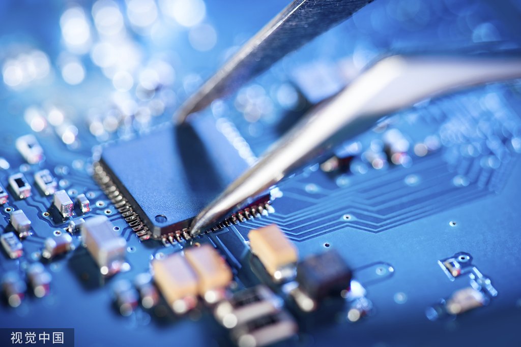
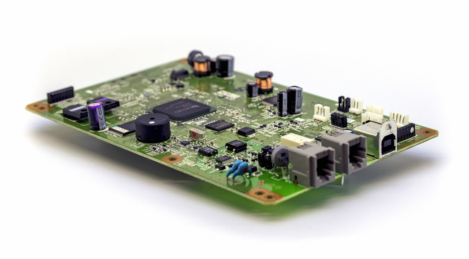
Printed Circuit Boards (PCBs) are fundamental components in modern electronic devices, providing the platform for electronic circuits. Understanding the materials that constitute PCBs is essential for grasping their functionality, performance, and applications in various industries.
Substrate Materials
The substrate is the foundation of a PCB, typically made from fiberglass-reinforced epoxy laminate known as FR4. This material provides the necessary structural integrity and insulates the conductive layers from each other. FR4 is preferred due to its excellent mechanical strength, low moisture absorption, and favorable electrical insulation properties.
Types of Substrates
1. FR4 (Flame Retardant 4): The most common substrate material, known for its durability and resistance to environmental stresses.
2. Polyimide: Used in flexible PCBs (flex PCBs), offering high thermal stability and flexibility, which is essential for applications requiring dynamic bending and high-temperature endurance.
3. Metal Core: Utilized in applications requiring efficient heat dissipation, such as LED lighting and power electronics. The metal core, usually aluminum or copper, helps in managing heat effectively.
Conductive Layer
The conductive layers in a PCB are typically made of copper. Copper is chosen for its excellent electrical conductivity, which ensures efficient signal transmission and power distribution across the board. The copper layers are laminated onto the substrate through a process called copper cladding.
Copper Thickness
The thickness of the copper layer can vary depending on the PCB’s application and requirements:
· Standard Copper (1 oz/ft²): Used in most consumer electronics.
· Heavy Copper (>3 oz/ft²): Utilized in high-power applications to handle greater current loads and improve thermal management.
Solder Mask
The solder mask is a protective layer applied over the copper traces to prevent short circuits, oxidation, and mechanical damage. It also helps in guiding the soldering process during component assembly by keeping the solder in the designated pads. The solder mask is typically green but can come in various colors like red, blue, or black for different visual requirements.
Silkscreen
The silkscreen layer is used to apply labels, symbols, and component designators on the PCB surface, aiding in the assembly and troubleshooting processes. The silkscreen ink is usually white, providing a clear contrast against the solder mask.
Surface Finish
The surface finish protects the exposed copper pads and ensures reliable soldering. Common types of surface finishes include:
· HASL (Hot Air Solder Leveling): An economical choice providing a good solderable surface.
· ENIG (Electroless Nickel Immersion Gold): Offers excellent surface planarity and long shelf life, ideal for fine-pitch components and surface mount technology (SMT).
· OSP (Organic Solderability Preservative): A lead-free option that maintains the copper’s solderability.
Advanced Materials
For specialized applications, advanced materials may be employed:
· Rogers Materials: Used in high-frequency and microwave PCBs, offering superior electrical performance at high frequencies.
· Ceramic: Provides high thermal conductivity and low expansion, suitable for high-temperature applications and aerospace.
Conclusion
The composition of PCB boards involves a combination of materials each serving a specific function to ensure the reliability and efficiency of the electronic devices they support. From the robust FR4 substrate and conductive copper layers to protective solder masks and advanced surface finishes, each material is carefully selected to meet the rigorous demands of modern electronics. Partnering with a trusted PCBA manufacturer like ArisenTec can further enhance the quality and performance of your PCBs. For more information on PCB manufacturing and custom design services, visit ArisenTec PCB.
Choosing the Right Wires for Breadboard Wiring: A Comprehensive Guide
Breadboards are a staple in electronic circuit building, offering flexibility and ease of use for both beginners and professionals. However, one of the most critical aspects of working with breadboards is selecting the right wires. The wires you choose can impact not only the functionality of your circuit but also its longevity and ease of…
How to Improve Heat Dissipation in PCB Design
Introduction As modern electronic devices become more complex and power-dense, heat dissipation has emerged as a critical factor that directly impacts device performance and reliability. Excessive junction temperatures in electronic systems can shorten the lifespan of components and lead to system failure. Thus, optimizing the PCB (Printed Circuit Board) design to improve heat dissipation is…
Manufacturing Process of Multilayer PCBs
Multilayer PCB manufacturing methods include the plated-through hole (PTH) and high-density interconnect (HDI) methods, both achieved by combining different processes to realize the circuit board structure. Currently, the most widely used method is the PTH method, which has been developed and refined over more than half a century. The PTH method is mature in terms…


