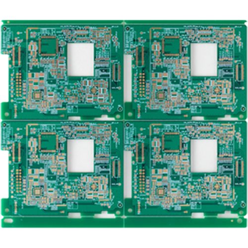
In the realm of electronic devices, multilayer Printed Circuit Boards (PCBs) are the unsung heroes. These complex assemblies form the foundation of most modern electronics, from the simplest gadgets to the most advanced computing systems. The process of manufacturing multilayer PCBs is a testament to the marvels of electronic engineering, involving a series of precise and controlled steps. Let’s explore this intricate process, highlighting the expertise of some of the best PCB manufacturers, including those in China, such as Arisentec, which has garnered global recognition for its quality and innovation.
The Genesis: PCB Design
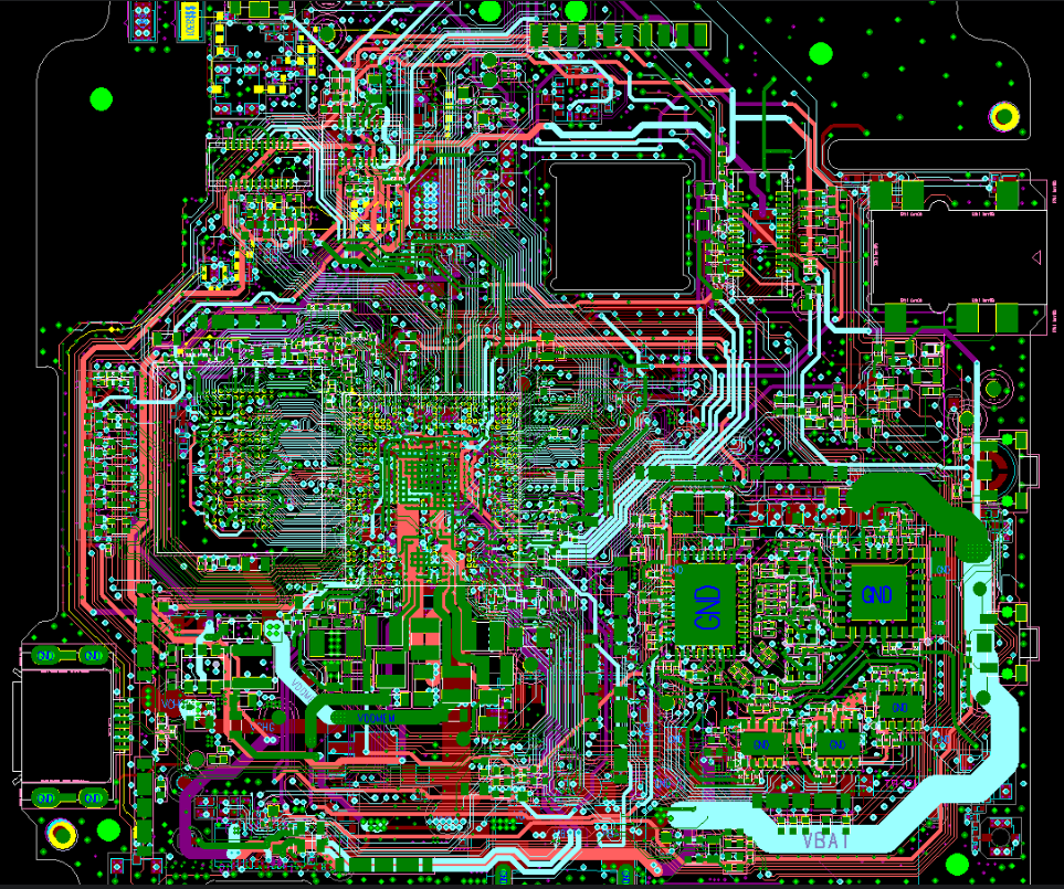
The creation of a multilayer PCB begins with an intricate dance of design and planning. Utilizing advanced PCB design services, engineers meticulously plot the layout of the board. This blueprint details the placement of components, the routing of multilayer traces, and the positioning of vias (the vertical connections between PCB layers). It’s a phase where foresight meets precision, ensuring that the final product is not only functional but also manufacturable with high efficiency.
The Core and the Layers
At the heart of the multilayer PCB is the core material, typically a robust type of fiberglass like FR4, which provides the necessary rigidity. This core is sandwiched between multiple layers of copper, separated by insulating materials known as prepreg, to prevent electrical shorts. The copper layers will soon be etched to form the circuitry that’s essential for the PCB’s function.
The Art of Etching
The etching process begins with the application of a photoresist to the copper layers, followed by a strategic exposure to light. This exposure is guided by a mask that imitates the circuit pattern. The photoresist that’s exposed to light hardens, while the rest is removed, revealing the copper that’s then etched away to create the intricate circuit patterns.
Lamination: The Binding Force
Quality control is paramount, as each layer is inspected for defects. Once approved, the layers are stacked, aligned, and laminated. This lamination process involves the application of heat and pressure, which melds the layers into a singular entity, ready for the next phase.
Drilling Down to Precision
Precision drilling follows, creating the vias that are crucial for the board’s functionality. These vias must align perfectly across all layers to ensure the integrity of the electrical connections.
Plating and Protection
Post-drilling, the board undergoes plating, where copper is deposited into the vias, solidifying the interlayer connections. Additional copper may be added to the surface to fortify the traces. The board is then coated with a solder mask, protecting the copper and preventing unwanted solder bridges during component assembly. A silkscreen layer is added last, providing essential markings for component placement.
Turnkey PCB Assembly: The Final Frontier
For full-service providers like Arisentec, the process extends into turnkey PCB assembly. This involves the meticulous sourcing of components, leveraging a vast network of suppliers and a comprehensive supply chain management system. The components are then placed and soldered onto the board, a process that can vary from reflow to wave soldering, depending on the requirements.
Testing: The Seal of Functionality
The final act in the PCB’s creation is rigorous testing. Each assembled PCB is subjected to a battery of electrical tests to confirm its functionality. This could range from simple in-circuit tests to complex functional verifications, ensuring that the final product meets the stringent standards required by the industry.
In Conclusion
The manufacturing of multilayer PCBs is a sophisticated process that demands expertise, precision, and a deep understanding of electronics. Companies like Arisentec offering comprehensive solutions that encompass PCB design, fabrication, and assembly. As the electronic industry continues to grow, the demand for quick turn PCB prototypes and fast PCB prototyping services will only increase, underscoring the critical role of PCB manufacturers in the global market.