Printed circuit board (PCB) is hailed by many people as the mother of electronic products. It is a key component of consumer electronics such as computers and mobile phones. It is widely used in medical, aviation, new energy, automotive and other industries. Almost every day we are in Experience the convenience brought by electronic products. Throughout the brief history of PCB development, every technological advancement directly or briefly affects all mankind. Today SPEA will tell you a brief history of PCB development.

PCB Enlightenment Stage (1900~1920s)
Before the birth of the PCB, any electronic device contained many wires, which not only get tangled together, take up a lot of space, but it is not uncommon for them to short out. The first to propose the concept of the PCB was the German inventor Albert Hansen. He pioneered the concept of using “wire” for telephone switching systems, metal foil is used to cut the line conductors, and then glued paraffin paper on the top and bottom of the line conductors, and set via holes at the crossings of the lines to realize the connection between different layers Electrical interconnection also lays a theoretical foundation for PCB manufacturing and development.
PCB development stages (1920s-1940s)
In 1925, Charles Ducas from the United States proposed an unprecedented idea of printing circuit patterns on insulating substrates, followed by electroplating to manufacture conductors for wiring. The term “PCB” came from this, and this The method simplifies the manufacture of electrical appliances.
In 1936, Paul Eisler was honored as the “Father of Printed Circuits” because he first published thin-film technology and developed the first printed circuit board for radios. The method he used is very similar to the method we use for printed circuit boards today. This method is called subtraction, and it removes unnecessary metal parts. Around 1943, his technological invention was widely used by the United States to manufacture proximity fuzes used in World War II. At the same time, the technology was widely used in military radios.
Commercialization and dissemination of PCB
In 1948, PCB ushered in a turning point for rapid development, and the United States officially recognized the invention of printed circuit boards for commercial use. By the 1950s, the U.S. Army had developed an automatic assembly process, which enabled mass production and made PCBs in electronics more widely used by consumers.
Rapid development stage (1970-1990):
Around the 1970s, another very important invention appeared – the IC (Integrated Circuit). The first microprocessor was actually invented by Jack Kilby in the late 50s, but it took him over a decade to share with Texas Instruments, which led to the development of the first integrated circuit. With the advent of the integrated circuit, and into the world of electronics manufacturing, the use of PCBs became mandatory.
In the 1970s, multi-layer PCB developed rapidly, pursuing higher precision and density, small holes with fine lines, high reliability, lower cost, and automated production. At that time, PCB design work was still done by hand. PCB Layout engineers used colored pencils and rulers to draw circuits on clear mylar. To improve drawing efficiency, they made several packaging templates and circuit templates for some common devices.
By the 1980s, PCBs were still drawn by hand, which of course was less dynamic, allowing only photos to be used to save and transfer designs. Computers and EDA (Electronic Design Automation) software then come into play to make the PCB design dynamic and incorporated into the PCB manufacturing machines. At the same time, compatible and lightweight gadgets, such as walkmans and cordless phones, were based on small PCBs, and surface mount technology (SMT) began to gradually replace through-hole mounting technology to become the mainstream at that time. It also entered the digital age and won People’s favor.
Mature stage (1990-21st century)
In the 1990s, electronic equipment continued to shrink, which also made PCBs for mechanical manufacturing more demanding. The Internet was also born and started a revolution that made the personal computer more and more popular all over the world. Cell phones were later introduced, and this technological leap would not have been possible without the advancement and minimization of PCB technology.
In the 2000s, PCBs became more complex with more functions while the size became smaller. Especially the multi-layer and flexible circuit PCB designs make these electronic devices more operable and functional, with small size and low cost PCB.
At the beginning of the 21st century, the emergence of smart phones promoted the development of HDI PCB technology. While retaining the laser-drilled micro-holes, stacked vias began to replace staggered vias, and combined with “any layer” construction technology, the final line width/line of HDI boards distance up to 40 μm.
This arbitrary layer method is still based on a subtractive process, and it is safe to say that for mobile electronics, most high-end HDIs are still using this technology. However, in 2017, HDI started to enter a new stage of development, starting to shift from subtractive processes to Process based on pattern plating.
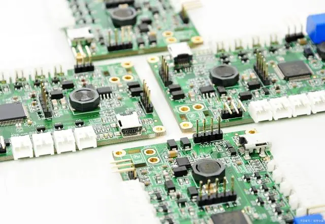
Nowadays, various types of printed circuit boards including rigid PCB, rigid-flex, multi-layer printed circuit board, and HDI PCB are widely used in the market, and the circuit board manufacturing industry is still making great strides after undergoing many evolutions Row. Future impact PCB is expected to go further in the following areas.