Choosing the Right Wires for Breadboard Wiring: A Comprehensive Guide
Breadboards are a staple in electronic circuit building, offering flexibility and ease of use for both beginners and professionals. However, one of the most critical
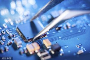
High-speed Printed Circuit Board (PCB) design is an intricate field of electrical engineering that focuses on designing PCBs capable of operating at high frequencies. These types of PCBs are crucial in modern electronics, where rapid signal processing and high data rates are essential. Unlike traditional PCB design, high-speed PCB design must account for the complexities of electromagnetic fields, signal integrity, and the physical limitations of the circuit materials. The evolution of this field has been driven by the demand for faster and more efficient electronic devices, leading to innovative methodologies and advanced materials.
The importance of high-speed PCB design cannot be overstated. It plays a pivotal role in the functionality and performance of a wide range of devices, from smartphones and computers to advanced communication systems and aerospace electronics. As technologies advance, the challenges and complexities in high-speed PCB design also grow, necessitating a deep understanding of electrical principles, materials science, and modern fabrication techniques.
At the heart of high-speed PCB design are the electrical characteristics that govern how signals behave on the board. These include impedance, capacitance, and inductance, which must be carefully managed to ensure signal integrity. Signal integrity is crucial in high-speed design, as it determines the quality and reliability of the signal being transmitted. High-speed signals, typically in the GHz range, are more prone to losses, reflections, and other distortions, making their management a core focus of the design process.
Understanding these electrical characteristics requires a deep dive into the physics governing high-speed signals.
As frequencies increase, the wavelength of signals becomes comparable to the dimensions of the PCB traces, leading to phenomena like signal reflections, impedance mismatches, and power dissipation. Designers must therefore consider the behavior of electromagnetic waves on the PCB and employ strategies like impedance matching and controlled impedance traces. This ensures that signals are transmitted with minimal loss and distortion, which is vital for maintaining the performance of high-speed electronic systems.
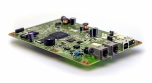
Selecting the right materials is critical in high-speed PCB design. The substrate material, for instance, must have a low dielectric constant and low loss tangent to minimize signal attenuation and dispersion. Common materials include FR4, Rogers, and Teflon, each with distinct properties suited for different frequency ranges and applications. Additionally, the choice of copper thickness, surface finish, and solder mask also plays a significant role in the performance of the high-speed PCB.
Component selection is equally important. High-speed designs often require components with minimal parasitic capacitance and inductance, as these can degrade signal integrity. Designers must also consider the package size and pinout of components, as these factors can affect trace routing and, consequently, signal performance. The challenge lies in balancing the electrical requirements with physical constraints and availability, making component selection a critical step in the design process.
When designing a high-speed PCB, trace layout and routing are paramount. Signal paths must be as short and direct as possible to reduce signal degradation. Designers employ techniques like differential signaling, where pairs of traces carry inverted signals, to mitigate electromagnetic interference (EMI) and cross-talk. Additionally, maintaining consistent trace impedance is essential to prevent reflections, requiring careful calculation and layout of trace widths and spacings.
Power integrity is another critical aspect. High-speed circuits often require stable and noise-free power delivery, necessitating the use of decoupling capacitors, power planes, and careful routing of power traces. Thermal management is also a significant consideration, as high-speed components can generate considerable heat. Effective thermal design, including the use of heat sinks, thermal vias, and careful component placement, is essential to ensure reliable operation under all conditions.
Simulation plays a crucial role in high-speed PCB design. Before physical prototypes are made, designers use software tools to model and analyze the behavior of signals on the PCB. These simulations help identify potential issues with signal integrity, cross-talk, EMI, and thermal performance. Tools like SPICE for circuit simulation and electromagnetic field solvers are commonly used for this purpose.
Once a design is finalized and a prototype is manufactured, extensive testing is necessary to ensure that the PCB performs as expected. This includes signal integrity testing, power integrity analysis, and thermal testing. Advanced equipment like Time Domain Reflectometers (TDR) and Vector Network Analyzers (VNA) are used to measure signal quality and impedance characteristics. The results from these tests guide further design iterations, ensuring that the final product meets all specifications and performance requirements.
One of the primary challenges in high-speed PCB design is addressing cross-talk and electromagnetic interference (EMI). As signal frequencies increase, the PCB traces act more like antennas, emitting and receiving electromagnetic waves. This can lead to unwanted coupling between traces, known as cross-talk, and can degrade signal integrity. Designers must employ techniques like proper trace spacing, shielding, and the use of ground planes to mitigate these effects.
Another challenge is balancing performance with manufacturability. High-speed PCBs often require precise fabrication techniques, which can increase costs and complexity. Designers must find a balance between achieving the desired electrical performance and ensuring that the PCB can be reliably and economically manufactured. This includes considerations for tolerances, material choices, and the complexities of multi-layer PCBs.
High-speed PCB design finds its application in a diverse range of industries. For instance, in telecommunications, high-speed PCBs are essential for routers, switches, and base stations, where they enable fast data transmission and processing. Another example is in the aerospace industry, where high-speed PCBs are used in satellite communication systems and avionics, requiring stringent performance and reliability standards.
A notable case study is the development of a high-speed PCB for a 5G communication system. This project required careful consideration of signal integrity at extremely high frequencies, material selection for
optimal performance, and innovative cooling solutions to manage the heat generated by high-speed components. The design team employed advanced simulation tools to model the electromagnetic behavior of the PCB, optimizing the layout for minimal signal loss and cross-talk. The final design not only met the stringent performance requirements but also adhered to industry standards for manufacturability and reliability, showcasing the intricate balance and expertise required in high-speed PCB design.
The future of high-speed PCB design is shaped by emerging technologies and evolving standards. One significant trend is the move towards even higher frequencies, such as those used in millimeter-wave applications, pushing the boundaries of material and design techniques. Another trend is the increasing integration of optical and electronic components, leading to hybrid PCBs that combine the best of both worlds for ultra-high-speed data transmission.
Furthermore, the development of new materials with better electrical properties is ongoing. For example, advanced composites and nano-materials offer the potential for higher performance and more compact designs. Additionally, as the Internet of Things (IoT) and edge computing continue to grow, there will be an increasing demand for high-speed PCBs that can operate efficiently in a wide range of environments, driving innovation in this field.
High-speed PCB design is a critical and ever-evolving field in the electronics industry. Its importance in the performance and reliability of modern electronic systems cannot be overstated. With advancements in technology, the challenges and complexities in high-speed PCB design are set to increase, requiring continuous learning and adaptation by designers. As we look to the future, the field of high-speed PCB design holds exciting possibilities, promising to push the limits of what’s possible in electronic design and functionality.
Arisentec, recognized as one of the best PCB manufacturers in China, plays a crucial role in the realm of high-speed PCB design. Their expertise in flex PCB manufacturing and quick turn PCB prototypes is particularly valuable for projects that demand rapid development and testing. This capability is essential for meeting the stringent performance and speed requirements in high-speed PCB applications.
Moreover, Arisentec’s comprehensive turnkey PCB assembly services, encompassing everything from PCB design to assembly, make them a preferred choice for complex high-speed PCB projects. Their integrated approach ensures precision and coordination throughout the manufacturing process, which is vital for the advanced electronic hardware design involved in high-speed PCBs. For more information about their services, visit https://arisentecpcb.com/

Arisentec is a leading PCB manufacturer based in Shenzhen, China, specializing in PCB design, fabrication, and assembly. Founded in 2011, they provide comprehensive solutions in various sectors like telecommunications, medical, industrial control, smart home, and IoT.
Breadboards are a staple in electronic circuit building, offering flexibility and ease of use for both beginners and professionals. However, one of the most critical
Introduction As modern electronic devices become more complex and power-dense, heat dissipation has emerged as a critical factor that directly impacts device performance and reliability.
Multilayer PCB manufacturing methods include the plated-through hole (PTH) and high-density interconnect (HDI) methods, both achieved by combining different processes to realize the circuit board

When designing PCBs, routing is essential. The quality of the routing affects the aesthetics, production cost, circuit performance, heat dissipation, and device optimization. This article

In PCB fabrication, the transition from a digital design to a physical product involves several crucial steps. One of the most important phases in this process

Programming a printed circuit board (PCB) involves loading firmware or software onto a microcontroller or processor embedded within the PCB. This process is crucial for