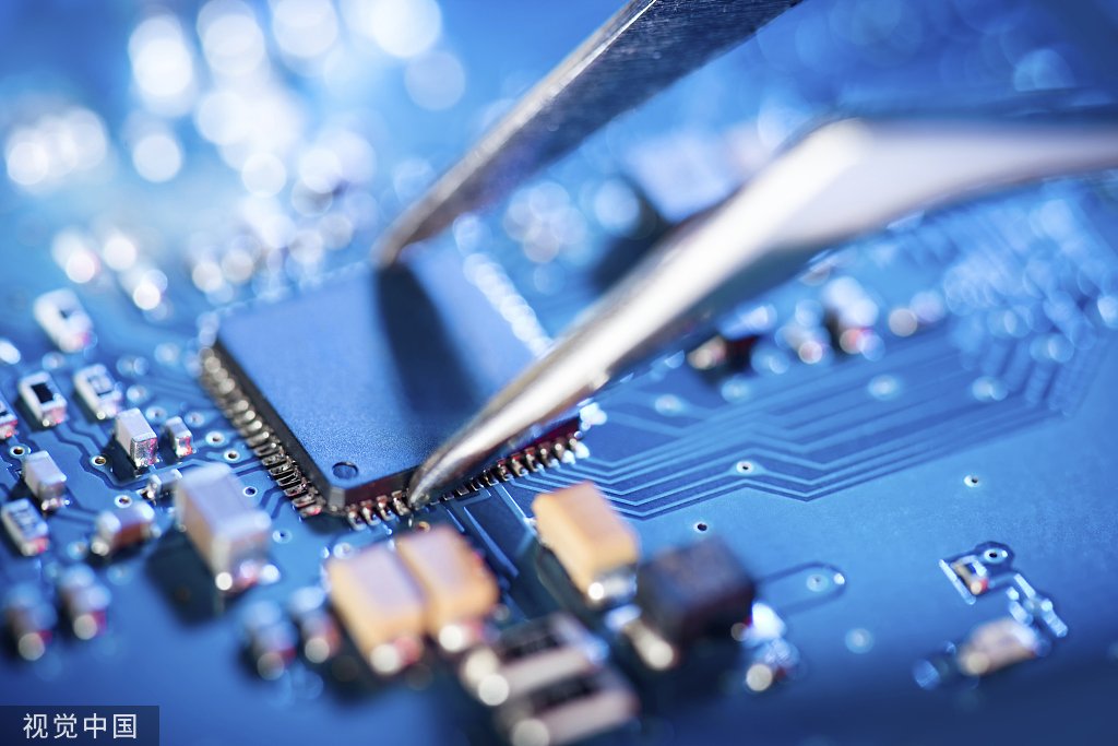
- Introduction to High-Power PCB Design
- Characteristics of High-Power PCBs
- Types of High-Power PCBs
- Design Features of High-Power PCBs
- Market Varieties of High-Power PCBs
- Safety Concerns in High-Power PCB Design
- Thermal Management Techniques
- Component Selection and Placement
- Advanced Design Techniques
- Power Distribution and Grounding Strategies
- Layering and Copper Thickness in High-Power PCBs
- PCB Manufacturing Processes for High-Power Boards
- Conclusion
Introduction to High-Power PCB Design
High-power Printed Circuit Boards (PCBs) stand as a cornerstone in the realm of modern electronics, catering to applications demanding high current and thermal resilience. Distinguished from their standard counterparts, these PCBs are designed to handle significantly higher electrical loads, making them indispensable in industrial, military, and high-tech applications. The essence of high-power PCB design lies in its ability to manage increased electrical stress while ensuring reliability and safety.
The development of high-power PCBs has been driven by the evolving demands of sophisticated electronic devices. As electronic components become more powerful, the need for PCBs that can sustain higher power levels without compromising performance or safety becomes paramount. This not only involves using materials that can withstand high temperatures but also entails intricate design techniques to manage the increased electrical and thermal loads. The growth of sectors like renewable energy, automotive electronics, and high-power computing further underscores the importance of these specialized PCBs.

Characteristics of High-Power PCBs
The primary characteristic that sets high-power PCBs apart is their use of heavy copper. Unlike standard PCBs, which typically feature copper layers ranging from 1/2 oz/ft² to 3 oz/ft², high-power boards may employ copper layers that are significantly thicker. This heavy copper enables the board to conduct higher currents while providing robust mechanical strength and significantly enhancing the PCB’s thermal management capabilities.
Another defining feature of high-power PCBs is their enhanced ability to resist thermal stress. These PCBs are often subjected to high operating temperatures for prolonged periods, making thermal resistance a critical factor. To address this, high-power PCBs incorporate advanced thermal management techniques, such as heat sinks, thermal vias, and specialized cooling layouts. These features help in dissipating the heat generated by high-power components, ensuring that the PCB maintains its performance and reliability even under extreme thermal conditions.

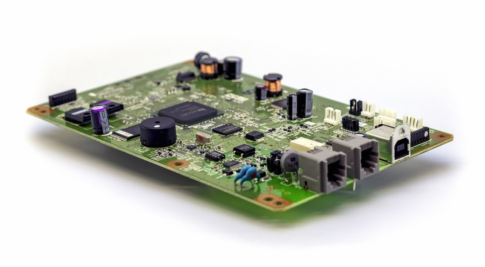
Types of High-Power PCBs
High-power PCBs come in various types, each tailored to specific applications and power-handling requirements. A common type is the double-sided PCB, which allows for component mounting on both sides, effectively doubling the available real estate for components. This design is particularly beneficial for compact devices where space is at a premium. The double-sided PCBs are a step up from single-layer boards, offering improved power handling and efficiency due to their expanded layout options.
Another significant category is the multi-layer PCB. These boards have at least three conductive layers, with some high-power applications requiring up to twelve or even more layers. The multi-layer design is pivotal for complex high-power applications, allowing for intricate routing and higher circuit densities. This design is instrumental in managing cross-layer electrical connections, which is essential for sophisticated high-power electronics.
Rigid-flex PCBs represent a blend of rigid and flexible board technologies. They consist of multiple layers of flexible substrate attached to one or more rigid boards. This combination allows for a design that can bend during use, which is crucial in space-constrained applications. The flexibility of these PCBs is not just physical; it extends to their functionality, enabling them to fit into unconventional spaces while providing robust electrical performance.
Design Features of High-Power PCBs
In high-power PCB design, the thickness and quality of the copper layers are paramount. These PCBs typically feature copper layers that are considerably thicker than those in standard PCBs, which is crucial for conducting higher currents without overheating. This increased thickness also contributes to the mechanical robustness of the PCB, supporting heavier components and providing strong connection points, which is particularly important in high-vibration environments or where physical stress is a concern.
Thermal management is another critical aspect of high-power PCB design. Efficient heat dissipation is vital to prevent component damage and ensure reliable operation. High-power PCBs often incorporate dedicated heat sinks, thermal vias, and conductive planes to manage heat. These components work together to transfer heat away from critical components and maintain a stable operating temperature. Additionally, the layout of high-power PCBs is designed to minimize hot spots and ensure uniform heat distribution across the board.
Market Varieties of High-Power PCBs
The market offers a diverse range of high-power PCBs, each tailored to specific industry requirements and applications. Among the popular varieties are those used in renewable energy systems, such as solar inverters and wind turbine controllers, where they handle high currents and operate in fluctuating temperature conditions. Another significant segment is automotive electronics, especially in electric and hybrid vehicles, where high-power PCBs are crucial for managing the high current demands of powertrain systems and battery management units.
In the realm of industrial applications, high-power PCBs are extensively used in power distribution systems and heavy machinery. The ability to handle high electrical loads makes them ideal for applications such as high-capacity power supplies, industrial motor controllers, and heating systems. Each of these applications places unique demands on the PCB, from high current capacity to enhanced thermal management, driving the development of specialized high-power PCB varieties.
Safety Concerns in High-Power PCB Design
Safety is a critical concern in high-power PCB design, primarily due to the high currents and temperatures involved. One of the primary considerations is ensuring the board can handle the thermal stresses without degradation or failure. This involves not only selecting materials with high thermal endurance but also designing the board layout to distribute heat evenly and incorporate effective cooling mechanisms.
Another major safety aspect is managing the risk of short circuits and electrical overloads. High-power PCBs often incorporate robust protection mechanisms, such as fuses and circuit breakers, to prevent damage in case of a fault. Additionally, careful layout and spacing of components are essential to prevent arcing and maintain electrical isolation, especially in applications where the board is exposed to high voltages.
Thermal Management Techniques
Effective thermal management is a cornerstone of high-power PCB design. As these boards handle significant electrical loads, they generate considerable amounts of heat, which must be dissipated efficiently to prevent damage and ensure reliability. One common technique is the use of heat sinks, which are attached to components that generate the most heat, such as power transistors or voltage regulators. These heat sinks help to dissipate the heat into the surrounding air, thus cooling the components.
Another critical technique is the use of thermal vias. These are small holes in the PCB filled or plated with a thermally conductive material, creating a path for heat to move from one side of the board to the other, often to a heat sink or thermal pad. Additionally, the design of the PCB layout itself plays a crucial role in thermal management. Strategic placement of components and power tracks helps to distribute heat evenly across the PCB, reducing hotspots and improving overall thermal performance.
Component Selection and Placement
Selecting the right components is crucial in high-power PCB design. Components must not only be able to handle the electrical requirements of the application but also withstand the thermal stresses they will be exposed to. This often means choosing components with higher current ratings and better thermal performance than would be required for lower-power applications.
The placement of these components on the PCB is just as important. High-power components should be evenly distributed to prevent localized hotspots. Components sensitive to heat should be placed away from heat-generating parts. Furthermore, the layout should consider the flow of high currents to minimize resistance and inductance, which can lead to additional heat generation and inefficiencies.
Advanced Design Techniques
In high-power PCB design, advanced techniques are employed to handle the unique challenges these boards present. One such technique is the use of thicker copper layers, which can carry higher currents without significant heat generation. This also contributes to the overall mechanical strength of the PCB, an important consideration in high-power applications.
Another advanced technique is differential etching, which allows for precise control of the thickness of the copper layers, enabling the design of more efficient power tracks. High-speed plating is also used to ensure that all layers of the PCB are uniformly plated with copper, essential for maintaining the integrity of the board under high-power conditions. These advanced manufacturing techniques are crucial in achieving the performance and reliability demanded by high-power applications.
Power Distribution and Grounding Strategies
In high-power PCBs, efficient power distribution and grounding are crucial for both performance and safety. Power distribution needs to be designed to minimize losses and ensure that each component receives a stable power supply under varying load conditions. This is often achieved by using thick copper traces or busbars for the main power paths, which reduce resistance and thus power loss.
Grounding in high-power PCBs is equally important and more complex. A well-designed grounding system reduces noise, minimizes electromagnetic interference (EMI), and enhances safety. In high-power applications, it’s often necessary to use multiple ground planes or separate grounding systems for different parts of the circuit, such as separating digital and analog grounds or providing isolated grounds for sensitive components.
Layering and Copper Thickness in High-Power PCBs
The layering and copper thickness in a high-power PCB play a pivotal role in its ability to conduct high currents and dissipate heat. Standard PCBs might use copper thicknesses around 1 to 2 ounces per square foot, but high-power PCBs often require thicker copper layers, sometimes up to 4 ounces per square foot or more. This increased thickness allows the PCB to carry higher currents without excessive heat buildup.
Moreover, the number of layers in a high-power PCB can significantly impact its performance. Multi-layer designs allow for better separation of power and ground planes, which can reduce EMI and improve thermal performance. Additionally, careful planning of the layer stack-up can help manage thermal stresses and ensure that heat is distributed evenly across the PCB.
PCB Manufacturing Processes for High-Power Boards
The manufacturing of high-power PCBs involves specialized processes to handle the thicker copper layers and ensure the integrity of the board under high stress. One such process is heavy copper etching, which requires precise control to achieve the desired copper thickness without compromising the trace definition or integrity.
Another key aspect is the lamination process, which needs to be carefully managed to avoid defects like delamination or warping, which are more likely with the thicker copper layers used in high-power PCBs. Additionally, high-power PCBs often undergo more rigorous testing and inspection processes to ensure they meet the higher performance and reliability standards required in high-power applications.
One-Stop Solution for PCB Assembly
-Arisentec offers comprehensive services for printed circuit board assembly, catering to a range of needs from prototypes to high-volume production.
-Advanced Manufacturing Capabilities: They specialize in advanced PCB technologies such as Every Layer Interconnect (ELIC), High Density Interconnect (HDI), and Rigid-Flex Circuits, showcasing their capacity for sophisticated high-power PCB design.
-Diverse Applications: Highlight Arisentec’s involvement in various industries like telecommunications, medical, smart home, and automotive, emphasizing their adaptability and expertise in different high-power PCB applications.
-Commitment to Innovation and Quality: Reflect on Arisentec’s dedication to continuous improvement promotes their goal of becoming the best PCB manufacturer china, emphasizing their role in pushing the boundaries of high-power PCB technology.
Incorporating these aspects will give a practical perspective on high-power PCB manufacturing and design, exemplified by a leading company in the field. For more detailed information, visit https://arisentecpcb.com/.
Conclusion
high-power PCBs are crucial in modern electronics, supporting a range of demanding applications with their robust design and efficient power management. This article has covered their key characteristics, types, design considerations, and the advanced manufacturing processes they require. As technology evolves, so will the demands on high-power PCBs, necessitating ongoing innovation in materials, design techniques, and thermal management. The future of high-power PCB design is set to play a pivotal role in the continued advancement of electronic technology, meeting the challenges of increasingly sophisticated and power-intensive applications.

Choosing the Right Wires for Breadboard Wiring: A Comprehensive Guide
Breadboards are a staple in electronic circuit building, offering flexibility and ease of use for both beginners and professionals. However, one of the most critical aspects of working with breadboards is selecting the right wires. The wires you choose can impact not only the functionality of your circuit but also its longevity and ease of…

How to Improve Heat Dissipation in PCB Design
Introduction As modern electronic devices become more complex and power-dense, heat dissipation has emerged as a critical factor that directly impacts device performance and reliability. Excessive junction temperatures in electronic systems can shorten the lifespan of components and lead to system failure. Thus, optimizing the PCB (Printed Circuit Board) design to improve heat dissipation is…

Manufacturing Process of Multilayer PCBs
Multilayer PCB manufacturing methods include the plated-through hole (PTH) and high-density interconnect (HDI) methods, both achieved by combining different processes to realize the circuit board structure. Currently, the most widely used method is the PTH method, which has been developed and refined over more than half a century. The PTH method is mature in terms…