For electronic equipment, a certain amount of heat will be generated during work, which will cause the internal temperature of the equipment to rise rapidly. If the heat is not dissipated in time, the equipment will continue to heat up, and the device will fail due to overheating. The reliability of electronic equipment Performance will drop. Therefore, it is very important to conduct a good heat dissipation treatment on the circuit board.
- Add copper foil for heat dissipation and copper foil for large-area power supply.
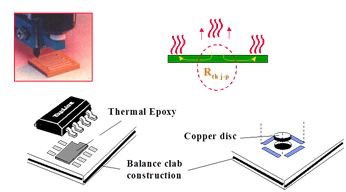
2. Thermal vias
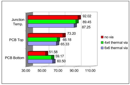
Thermal vias can effectively reduce the junction temperature of the device, improve the uniformity of temperature in the thickness direction of the single board, and provide the possibility to adopt other heat dissipation methods on the back of the PCB. Through simulation, it is found that compared with no thermal vias, thermal vias with a thermal power consumption of 2.5W, a pitch of 1mm, and a 6×6 center design can reduce the junction temperature by about 4.8°C, while the temperature difference between the top and bottom surfaces of the PCB Reduced from the original 21°C to 5°C. After changing the thermal via array to 4×4, the junction temperature of the device increased by 2.2°C compared with 6×6, which is worth noting.
3. Copper is exposed on the back of the IC, reducing the thermal resistance between the copper skin and the air
4. PCB layout
Requirements for high-power, heat-sensitive devices.
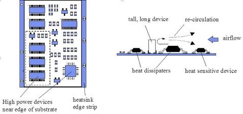
a. Thermally sensitive devices are placed in a cold wind area.
b. The temperature detection device is placed in the hottest position.
c. Devices on the same printed board should be arranged in partitions according to their calorific value and heat dissipation degree as far as possible. Devices with small calorific value or poor heat resistance (such as small signal transistors, small-scale integrated circuits, electrolytic capacitors, etc.) At the top of the cooling airflow (inlet), devices with high heat generation or good heat resistance (such as power transistors, large-scale integrated circuits, etc.) are placed at the most downstream of the cooling airflow.
d. In the horizontal direction, the high-power devices are arranged as close as possible to the edge of the printed board to shorten the heat transfer path; in the vertical direction, the high-power devices are arranged as close as possible to the top of the printed board in order to reduce the temperature of other devices when these devices are working. Impact.
e. The heat dissipation of printed boards in the equipment mainly depends on air flow, so the air flow path should be studied during design, and the components or printed circuit boards should be reasonably configured. When the air flows, it always tends to flow where the resistance is small, so when configuring devices on the printed circuit board, avoid leaving a large airspace in a certain area. The configuration of multiple printed circuit boards in the whole machine should also pay attention to the same problem.
f. Devices that are sensitive to temperature are best placed in the area with the lowest temperature (such as the bottom of the device). Do not place it directly above the heating device. Multiple devices are best arranged staggered on the horizontal plane.
g. Arrange the devices with the highest power consumption and the largest heat generation near the best heat dissipation position. Do not place devices with high heat generation on the corners and edges of the printed board unless there is a heat sink near it. When designing the power resistor, choose a larger device as much as possible, and make it have enough heat dissipation space when adjusting the layout of the printed board