Designing a custom keyboard PCB (Printed Circuit Board) is a detailed process that allows you to create a keyboard tailored to your specific needs. Whether you want a unique layout, special features, or a custom aesthetic, this guide will walk you through the key steps in designing your own keyboard PCB.
Understanding the Basics of Keyboard PCB Design
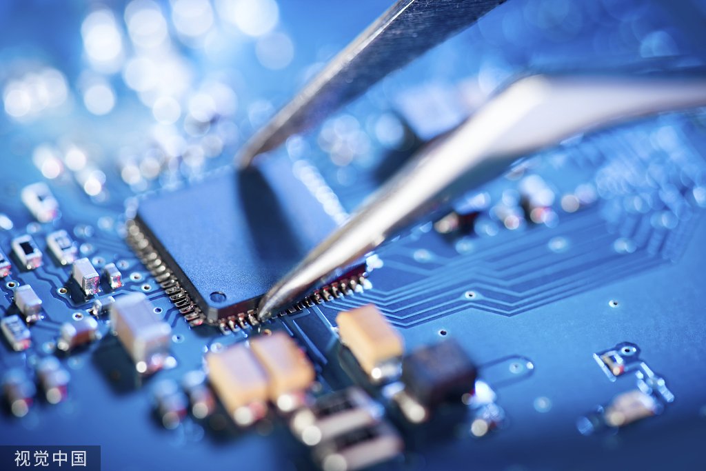
A keyboard PCB is the foundation of any keyboard, housing all the electrical connections required for it to function. Each key on the keyboard corresponds to a switch, and these switches are soldered to the PCB. The PCB connects to a computer via a microcontroller, which translates key presses into data.
The design process involves several stages, including layout design, switch placement, routing, and ensuring proper electrical connections. Additionally, it’s crucial to consider the printed circuit board cost and manufacturability if you plan on producing the keyboard in larger quantities.
Planning Your Keyboard Layout
The first step is to plan your keyboard layout. This involves determining the number of keys, the size and shape of the keyboard, and the placement of each key. Many designers use keyboard design tools to visualize the layout.
When planning, consider the type of switches you’ll use, as different switches have varying dimensions and mounting styles. Ensure your PCB design accommodates these switches, allowing for proper alignment and secure mounting.
Choosing the Right Software for PCB Design
After finalizing the layout, choose a PCB design software. There are several options, from beginner-friendly tools to advanced programs used by professional pcba manufacturers. Popular choices include KiCad, Eagle, and Altium Designer.
The software should allow you to import your layout and place components like Allegro, Pads and Mentor Expedition. It should also support creating a schematic that outlines the electrical connections between components, ensuring the keyboard functions correctly.
Designing the Schematic
The schematic is a blueprint showing how all the components on your PCB will be connected. This includes the microcontroller, switches, diodes (for anti-ghosting), resistors, and capacitors.
Each switch is connected to the microcontroller through a matrix of rows and columns, which allows the microcontroller to detect key presses. It’s crucial to ensure that your schematic accurately represents this matrix and that all connections are correct.
Routing the PCB
Routing the PCB involves placing the copper traces that carry electrical signals between components. Proper routing is essential for signal integrity and overall functionality.
Keep traces as short and direct as possible, and avoid crossing them to prevent signal interference. Pay attention to the placement of the microcontroller and USB connector for easy computer connection.
Additional Design Considerations
When designing your keyboard PCB, you may also consider using a flex PCB stiffener. A flex circuit stiffener adds mechanical support to flexible circuits, which can be useful in designs requiring extra durability.
Another important aspect is the power supply. For wireless keyboards, design the PCB to support battery power, including components like a battery connector and power management circuitry.
Prototyping and Testing
After completing your design, the next step is prototyping. Companies like ArisenTec offer pcb prototyping services that can produce a small batch of your custom PCB. Prototyping is crucial to verify that your design works as intended and to identify potential issues.
During testing, focus on key functionality, microcontroller performance, and overall electrical integrity. If issues arise, revise the design and create a new prototype.
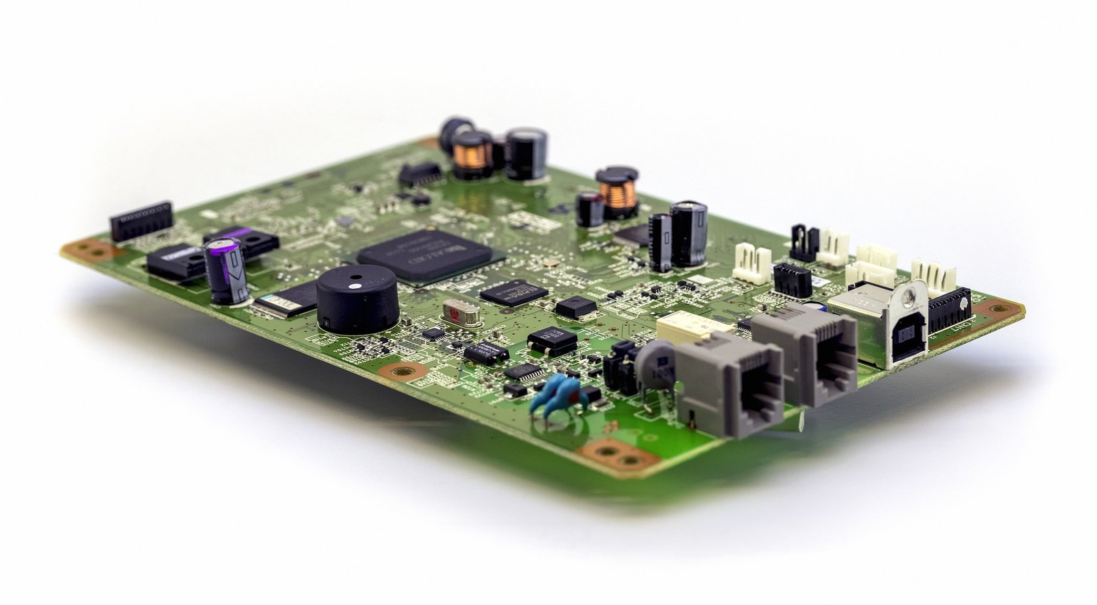
Manufacturing Your Keyboard PCB
After successful prototyping, you can move on to manufacturing. Choosing the right pcba manufacturer is key to ensuring the quality and performance of your keyboard. ArisenTec, for example, offers comprehensive services that include full turnkey PCB assembly, where they handle everything from component sourcing to assembly, ensuring a high-quality final product.
Consider factors like pcb assembly cost and lead time when selecting a manufacturer. A reliable partner like ArisenTec can streamline the process and deliver exceptional results.
Final Assembly and Customization
Once your PCBs are manufactured, proceed with the final assembly. This involves soldering the switches onto the PCB, installing the microcontroller, and assembling the keyboard case. You can also customize the keyboard with unique keycaps, backlighting, or other features to create a truly personalized product.
In conclusion, designing your own keyboard PCB is a complex process that requires careful planning, design, and testing. By following these steps and partnering with a trusted pcba manufacturer like ArisenTec, you can create a high-quality custom keyboard that meets your exact specifications.

Choosing the Right Wires for Breadboard Wiring: A Comprehensive Guide
Breadboards are a staple in electronic circuit building, offering flexibility and ease of use for both beginners and professionals. However, one of the most critical aspects of working with breadboards is selecting the right wires. The wires you choose can impact not only the functionality of your circuit but also its longevity and ease of…

How to Improve Heat Dissipation in PCB Design
Introduction As modern electronic devices become more complex and power-dense, heat dissipation has emerged as a critical factor that directly impacts device performance and reliability. Excessive junction temperatures in electronic systems can shorten the lifespan of components and lead to system failure. Thus, optimizing the PCB (Printed Circuit Board) design to improve heat dissipation is…

Manufacturing Process of Multilayer PCBs
Multilayer PCB manufacturing methods include the plated-through hole (PTH) and high-density interconnect (HDI) methods, both achieved by combining different processes to realize the circuit board structure. Currently, the most widely used method is the PTH method, which has been developed and refined over more than half a century. The PTH method is mature in terms…