Choosing the Right Wires for Breadboard Wiring: A Comprehensive Guide
Breadboards are a staple in electronic circuit building, offering flexibility and ease of use for both beginners and professionals. However, one of the most critical
AC to DC conversion is a fundamental process in modern electronics, where alternating current (AC) from the power grid is converted into direct current (DC) for use in electronic devices. This conversion is essential because most electronic components require DC for their operation. The process involves two key stages: rectification and filtering. In the rapidly evolving field of electronics, the role of specialized PCB design services and quick turn PCB prototypes has become increasingly crucial. These resources empower designers and engineers to rapidly develop and refine their concepts, setting a solid foundation for the advanced design work that follows.Rectification converts the AC into a pulsating DC signal, and filtering smooths out this signal to produce a steady DC output.
The efficiency of this conversion process largely depends on the type of rectifier used. There are two main types: half-wave and full-wave. A half-wave rectifier allows only one half of the AC cycle to pass through, resulting in significant energy loss and inefficiency. On the other hand, full-wave rectifiers enable both halves of the AC cycle to pass, significantly improving efficiency and providing a smoother DC output. This choice impacts the overall performance of the PCB design for AC to DC converters.
When designing a PCB for an AC to DC converter, several key factors must be considered to ensure efficient and reliable operation. First and foremost is component placement. Strategic positioning of components on the PCB can significantly influence the converter’s noise levels and heat dissipation. Ideally, components should be arranged to minimize the length of electrical traces, reducing the likelihood of electromagnetic interference and signal loss.
Another crucial aspect is the trace width and the thickness of the copper layer on the PCB. These must be carefully calculated to handle the expected current without overheating. This involves understanding the maximum current load and ensuring that the trace width can accommodate this without excessive heat buildup. Additionally, a solid ground plane is vital for minimizing noise and interference, offering a low-impedance path for the return current. Navigating the complexities of PCB layout for AC to DC converters often calls for the expertise provided by dedicated PCB layout services. Their involvement is particularly beneficial in optimizing component placement and trace routing, which are pivotal in achieving an efficient and reliable converter.This, combined with proper heat management strategies like the placement of heat sinks and careful positioning of heat-generating components, can significantly enhance the converter’s performance.
The choice of components in an AC to DC converter PCB layout is crucial for its functionality and efficiency. Diodes play a pivotal role in the rectification process. Rectifier diodes are typically used due to their ability to handle high currents and voltages. Schottky diodes are also favored in some designs for their low forward voltage drop and fast switching capabilities, which enhance the overall efficiency of the conversion process.
Capacitors are equally important in an AC to DC converter. They are used to filter out the AC ripple voltage and stabilize the DC output. Electrolytic capacitors are commonly chosen for their high capacitance values, making them ideal for smoothing out fluctuations in the DC output. Ceramic capacitors, known for their low Equivalent Series Resistance (ESR) and high-frequency response, are often used to supplement electrolytic capacitors, providing a more stable and reliable DC output.
Transformers, meanwhile, are employed to step down the AC input voltage to a more manageable level before rectification. Center-tapped transformers are commonly used, offering a reference point for the rectifier diodes, which is essential for stable operation. Toroidal transformers are also popular in compact designs due to their high efficiency and minimal electromagnetic interference.
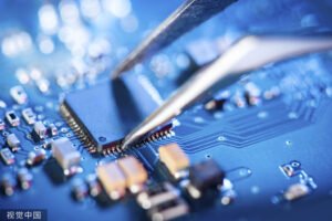
In the realm of microcontroller PCB design, the importance of selecting the right components cannot be overstated. Microcontrollers, as the brains of the PCB, require careful integration with other components to ensure smooth operation. For designers who might not have the bandwidth to delve into these complexities, utilizing professional PCB design services can be a valuable asset. These services often extend to helping choose the right microcontroller and other components, ensuring that the entire PCB functions cohesively.
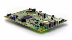
Moreover, for those embarking on new PCB board projects, especially in the realm of electronic hardware design, the partnership with a PCB manufacturer, particularly one based in China, can offer numerous benefits. These manufacturers often provide not just production services but also valuable insights into component selection based on their extensive experience. Their involvement can be pivotal in ensuring that the final design is both efficient and cost-effective.
Effective layout design is pivotal in maximizing the performance and reliability of an AC to DC converter. The placement of components on the PCB must be done with precision, ensuring logical and organized arrangement for efficient current flow and minimized signal loss. This organization aids in reducing noise and electromagnetic interference, crucial for maintaining the integrity of the converted signal.
Trace routing is another critical aspect of layout design. Traces should be as short as possible to reduce resistance and inductance. This is particularly important for high-frequency signals, which are more prone to interference and loss. Careful routing can greatly enhance the efficiency and stability of the converter. Grounding is also a vital consideration. A well-designed grounding system, including a solid ground plane, is essential for stabilizing the circuit and minimizing noise and interference. This aspect is often overlooked but can significantly impact the overall performance of the converter.
When it comes to laying out the PCB, one cannot underestimate the importance of pcb layout services, especially for complex designs involving multiple layers or intricate trace routing. These services are crucial in transforming a conceptual electronic hardware design into a tangible and functional printed circuit board prototype. With the advent of fast PCB prototyping services, designers can now quickly iterate their designs, making necessary adjustments based on real-world testing and feedback.
For those seeking a quick turn pcb prototypes, it’s important to work with a provider that understands the nuances of rapid prototyping. This approach is invaluable in accelerating the development cycle, allowing designers to test and refine their PCBs in a real-world context swiftly. This rapid prototyping not only speeds up the development process but also enhances the overall quality of the final product, as it allows for more iterative testing and refinement before mass production.
After completing the PCB layout, rigorous testing is essential to ensure the AC to DC converter operates as intended. Initial tests involve verifying the input voltage with a multimeter, ensuring compatibility with the converter’s specifications. Subsequent tests include connecting a load to the converter’s output, measuring the output voltage for stability, and checking the ripple voltage using an oscilloscope. Additionally, assessing the converter’s efficiency with a power meter is crucial to ensure it falls within the desired range.
Despite thorough testing, issues may arise. Common problems include overheating, often due to inadequate cooling or a faulty component, and output voltage fluctuations, potentially caused by defective capacitors or inductors. In some cases, there might be no output voltage, indicating a blown fuse or a faulty rectifier. Overloading issues can also occur if the converter is subjected to a load beyond its capacity. Identifying and addressing these issues is crucial for the successful application of the converter in various electronic devices.
Designing an AC to DC converter PCB is a complex task that requires careful consideration of various factors, including component selection, layout design, and testing procedures. By adhering to best practices in each of these areas, designers can ensure that their converters operate efficiently and reliably. The journey of designing an effective AC to DC converter is greatly enhanced by the support of experienced PCB design services and the availability of fast PCB prototyping.
These resources not only streamline the development process but also ensure a higher standard of performance and reliability in the final product, reflecting the cutting-edge nature of contemporary electronic hardware design. meeting the demands of modern electronic devices. This guide aims to provide a comprehensive overview of these considerations, aiding designers in creating effective and robust AC to DC converters.

Arisentec is a leading PCB manufacturer based in Shenzhen, China, specializing in PCB design, fabrication, and assembly. Founded in 2011, they provide comprehensive solutions in various sectors like telecommunications, medical, industrial control, smart home, and IoT. Arisentec offers a range of services, including high mix low volume and high volume PCB production, Every Layer Interconnect (ELIC), High Density Interconnect (HDI), and Rigid-Flex Circuits.
Breadboards are a staple in electronic circuit building, offering flexibility and ease of use for both beginners and professionals. However, one of the most critical

Introduction As modern electronic devices become more complex and power-dense, heat dissipation has emerged as a critical factor that directly impacts device performance and reliability.
Multilayer PCB manufacturing methods include the plated-through hole (PTH) and high-density interconnect (HDI) methods, both achieved by combining different processes to realize the circuit board

When designing PCBs, routing is essential. The quality of the routing affects the aesthetics, production cost, circuit performance, heat dissipation, and device optimization. This article

In PCB fabrication, the transition from a digital design to a physical product involves several crucial steps. One of the most important phases in this process

Programming a printed circuit board (PCB) involves loading firmware or software onto a microcontroller or processor embedded within the PCB. This process is crucial for