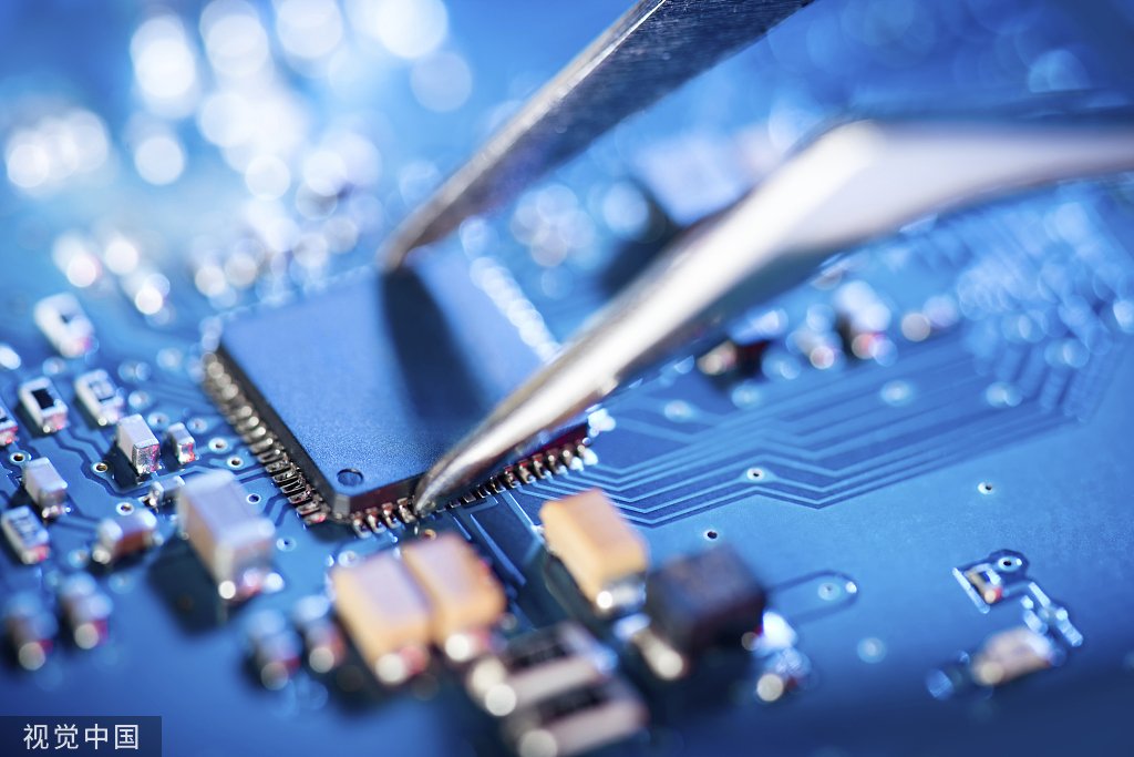
Calculating the current-carrying capacity of vias in printed circuit boards (PCBs) is essential to ensure that the electrical pathways in a circuit can handle the required load without overheating or failure. At ArisenTec, we understand the critical importance of this calculation in maintaining the reliability and performance of advanced PCBs. This article outlines the process of determining a via’s current-carrying capacity, considering the key factors involved.
1. Understanding the Structure of a PCB Via
A via is a small, cylindrical hole drilled through the layers of a PCB, typically plated with copper, which allows electrical connections between different layers of the board. The ability of a via to carry current depends largely on its size, the thickness of the copper plating inside it, and the ability of the surrounding PCB material to dissipate heat.
· Via Diameter (D): The diameter of the drilled hole in the PCB.
· Plating Thickness (T): The thickness of the copper layer that lines the inside of the via.
· Via Length (L): This is essentially the thickness of the PCB since the via usually passes through the entire board.
2. Importance of Thermal Management
The current flowing through a via generates heat due to electrical resistance. The capacity of the via to carry current without overheating depends on how effectively this heat can be dissipated. Key factors include:
· Thermal Conductivity of PCB Materials: Materials with higher thermal conductivity will dissipate heat more efficiently, allowing the via to carry more current.
· Ambient Temperature: The surrounding temperature plays a significant role; higher ambient temperatures reduce the via’s ability to carry current, as it starts at a higher baseline temperature.
3. Using Empirical Formulas and IPC Standards
The IPC-2221 standard provides widely accepted guidelines and empirical formulas for calculating the current-carrying capacity of PCB vias. One commonly used formula is:

Where:
· I is the current-carrying capacity in amperes (A).
· K is a constant that varies based on the desired temperature rise and the environmental conditions. For a typical 10°C temperature rise, K is approximately 0.048.
· D is the via diameter in mils (1 mil = 0.001 inches).
· T is the thickness of the copper plating inside the via, also in mils.
This formula provides a reasonable estimate of the current capacity. However, actual conditions may require adjustments, especially in more complex or demanding applications.
4. Considerations for Multiple Vias and PCB Layout
When multiple vias are used in parallel to carry current, the total current capacity is distributed among them. It is crucial to ensure that the vias are properly spaced to facilitate effective heat dissipation and avoid creating hot spots on the PCB. In high-current applications, vias may be filled or plugged with conductive materials to enhance both thermal and electrical performance.
The PCB layout must also consider the placement of vias to optimize current flow and minimize impedance. Properly designed PCB layouts will ensure that vias can handle the expected current load while maintaining the integrity of the board’s electrical performance.
5. Simulation and Testing
While empirical formulas and standards offer a solid foundation, they are often supplemented by simulations using advanced PCB design software. These simulations account for the specific layout of the PCB, the configuration of the vias, and the materials used, providing a more accurate assessment of current-carrying capacity.
Additionally, testing prototypes under realistic operating conditions is essential. This testing validates the calculated current-carrying capacity and ensures that the vias can handle the actual loads without failure.
6. Conclusion
At ArisenTec, ensuring that the vias in your PCB design can safely and effectively carry the required current is a top priority. By combining industry standards, precise calculations, advanced simulations, and thorough testing, we deliver PCBs that are both reliable and high-performing. Whether you require custom designs or turnkey solutions, ArisenTec is committed to providing PCBs that meet the highest standards of quality and durability.
For more information about our PCB manufacturing services, visit ArisenTec.

Choosing the Right Wires for Breadboard Wiring: A Comprehensive Guide
Breadboards are a staple in electronic circuit building, offering flexibility and ease of use for both beginners and professionals. However, one of the most critical aspects of working with breadboards is selecting the right wires. The wires you choose can impact not only the functionality of your circuit but also its longevity and ease of…

How to Improve Heat Dissipation in PCB Design
Introduction As modern electronic devices become more complex and power-dense, heat dissipation has emerged as a critical factor that directly impacts device performance and reliability. Excessive junction temperatures in electronic systems can shorten the lifespan of components and lead to system failure. Thus, optimizing the PCB (Printed Circuit Board) design to improve heat dissipation is…

Manufacturing Process of Multilayer PCBs
Multilayer PCB manufacturing methods include the plated-through hole (PTH) and high-density interconnect (HDI) methods, both achieved by combining different processes to realize the circuit board structure. Currently, the most widely used method is the PTH method, which has been developed and refined over more than half a century. The PTH method is mature in terms…