- The PCB of a motherboard is usually 4-layered.
- Copper Tracing Process
- I. Wire Width and Current
- II. What Frequency is Considered High-Speed for a Board?
- III. PCB Stacking and Layering
- IV.Impedance Matching
- V. Power and Ground Routing Considerations
- VI. Principles of Printed Circuit Board Design and Anti-interference Measures
- VII. Design Techniques and Tips for Efficient PCB Auto-routing
- In conclusion
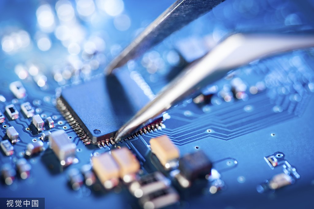
PCB stands for Printed Circuit Block, which is essentially a printed circuit board used for inserting electronic components, serving as a base with circuits. By employing a printing method to apply anti-corrosion circuit patterns on a copper-plated base and then etching away the excess, the circuit paths are created.
PCBs can be categorized into single-sided, double-sided, and multilayer boards.
Various electronic components are integrated onto the PCB. On the most basic single-sided PCBs, components are concentrated on one side, while the wiring is on the other. This necessitates drilling holes in the board so that component leads can pass through to the other side, where they are soldered.
Thus, the two sides of such a PCB are referred to as the Component Side and the Solder Side, respectively. A double-sided board can be seen as two single-sided boards bonded back-to-back, with electronic components and traces on both sides.
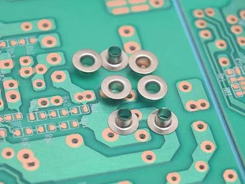
Sometimes, it’s necessary to connect a trace from one side of the board to the other, which is achieved through vias. Vias are small metal-filled or coated holes in the PCB that allow connections between traces on both sides.
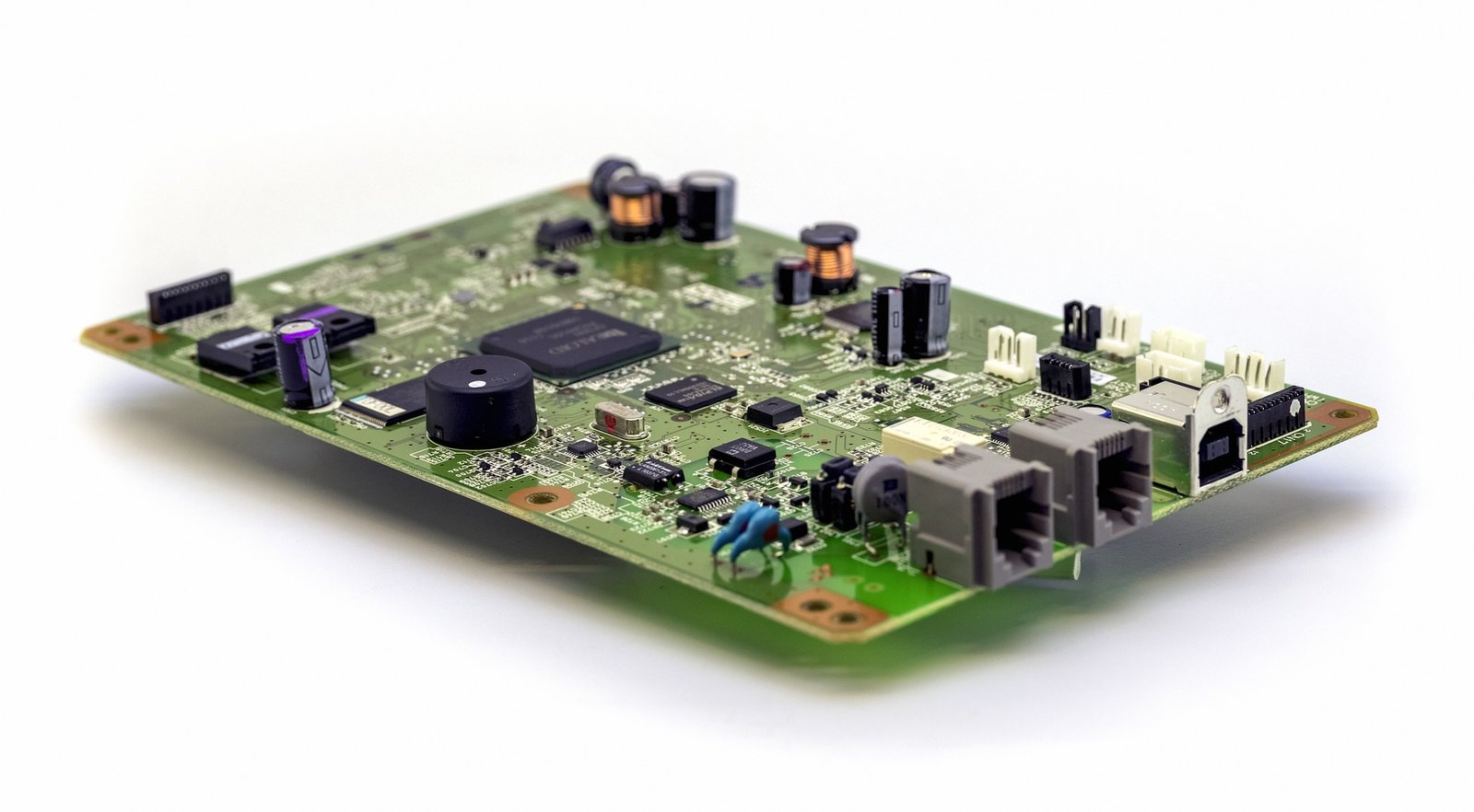
Nowadays, many computer motherboards use 4-layer or even 6-layer PCBs, while graphics cards typically use 6-layer PCBs. High-end graphics cards, like the NVIDIA GeForce 4 Ti series, utilize 8-layer PCBs, illustrating the concept of multilayer PCBs.
In multilayer PCBs, connecting circuits across different layers is also facilitated by vias. Since these are multilayer PCBs, sometimes vias do not need to penetrate the entire board; such vias are called buried vias and blind vias because they only go through several layers.
Blind vias connect some internal PCB layers to surface layers without going through the entire board. Buried vias connect only internal layers and are not visible from the surface. In multilayer PCBs, entire layers are directly connected to the ground or power supply.
Therefore, layers are designated as Signal, Power, or Ground layers. If a PCB’s components require different power supplies, such PCBs typically have more than two layers dedicated to power and ground.
The more layers a PCB has, the higher its cost. However, using more layers helps stabilize signal integrity.
The process of professional PCB production is quite complex. Taking a 4-layer PCB as an example:
The PCB of a motherboard is usually 4-layered.
During manufacturing, the middle two layers are each processed through pressing, cutting, etching, and electroplating. These four layers are the component layer, power layer, ground layer, and solder mask layer. These layers are then pressed together to form the PCB of a motherboard.
Next, holes are drilled, and vias are made. After cleaning, the outer layers’ traces are printed, copper is laid, etching is done, followed by testing, solder mask application, and silk screening.
Finally, the whole PCB (containing many motherboard units) is stamped into individual motherboard PCBs, which are then tested and vacuum-packed.
If the copper foil is not properly applied during the PCB manufacturing process, it can lead to adhesion issues, potentially hiding short circuits or creating capacitive effects (leading to interference).
Attention must also be paid to the vias. If a hole is not drilled precisely in the center but off to one side, it can lead to uneven matching or potential short circuits or poor grounding by contacting the middle power layer or ground layer.
Copper Tracing Process
The first step in production is to establish the connections between components.
A negative transfer method is used to transfer the working negative image onto the metal conductor. This technique involves covering the entire surface with a thin layer of copper foil and eliminating the excess.
Additive transfer, a less commonly used method, involves applying copper only where needed, but we won’t go into detail here.
Positive photoresist is made from a photosensitive material that dissolves under light. There are many ways to apply photoresist to the copper surface, but the most common method involves heating it and rolling it over the surface containing photoresist.
It can also be applied in liquid form, but dry film provides higher resolution and can create finer lines. The photomask is just a template for the PCB layers.
Before exposing the photoresist to UV light, the photomask prevents certain areas from being exposed. These covered areas will become the traces. After developing the photoresist, the other bare copper parts are etched.
The etching process can involve immersing the board in an etching solution or spraying the solution onto the board. Common etching solutions include ferric chloride. After etching, the remaining photoresist is removed.
I. Wire Width and Current
Generally, the width should not be less than 0.2mm (8mil). On high-density, high-precision PCBs, the spacing and line width are typically 0.3mm (12mil). When the thickness of the copper foil is around 50um, a wire width of 1~1.5mm (60mil) equals 2A.
A common ground is generally 80mil, and more attention should be paid in applications with microprocessors.
II. What Frequency is Considered High-Speed for a Board?
A signal is considered high-speed when its rise/fall time is < 3~6 times the signal transmission time.
For digital circuits, the key is the steepness of the signal’s edges, i.e., the rise and fall times.
According to the theory from a very classic book, “High-Speed Digital Design,” a signal is high-speed if it rises from 10% to 90% in less than six times the wire delay — meaning an 8KHz square wave signal, as long as the edges are steep enough, is considered a high-speed signal, requiring the use of transmission line theory in wiring.
III. PCB Stacking and Layering
Multilayer printed boards have better electromagnetic compatibility (EMC) design, allowing the printed board to meet electromagnetic compatibility and sensitivity standards during normal operation. Correct stacking helps with shielding and suppression of EMI. In multilayer printed board layering and stacking, the following basic principles are generally followed:
1) The power plane should be as close to the ground plane as possible and should be below it;
2) The wiring layer should be arranged adjacent to the plane layer;
3) The impedance of the power and ground layers should be the lowest;
4) Form striplines in the middle layers and microstrip lines on the surface. The two have different characteristics;
5) Important signal lines should be close to the ground layer.
A very important advantage of multilayer boards over conventional double-layer and single-layer boards is that signal lines and power can be distributed on different layers, improving signal isolation and anti-interference performance.
However, many engineers still find the layering and stacking of PCBs challenging, taking the commonly used 4-layer board as an example.
Four-Layer Board Stacking Orders (The advantages and disadvantages of each are explained below)
First Scenario:
This should be the best scenario among four-layer boards.
Because the outer layer is a ground layer, it provides EMI shielding, and the power layer can be very close to the ground layer, resulting in a lower internal resistance of the power supply, achieving the best results.
But the first scenario is not suitable for boards with high density because it cannot ensure the integrity of the first layer ground, worsening the second layer signal.
Additionally, this structure is not suitable for boards with high overall power consumption.
Second Scenario:
This is the most commonly used method.
It is also not suitable for high-speed digital circuit design from a board structure perspective because it is difficult to maintain low power supply impedance.
Taking a board with 2mm as an example: For Z0=50ohm, with a line width of 8mil and copper foil thickness of 35μm, the distance between the signal layer and the ground layer is 0.14mm, while the distance between the ground layer and the power layer is 1.58mm, significantly increasing the internal resistance of the power supply.
In this structure, since radiation is towards space, a shielding plate is needed to reduce EMI.
Third Scenario:
The signal quality on the S1 layer is the best, followed by S2, which provides EMI shielding, but the power impedance is larger.
This board can be used in situations where the entire board consumes a lot of power and the board is a source of interference or is close to a source of interference.
Note: S1 is the first signal wiring layer, S2 is the second signal wiring layer; GND is the ground layer, POWER is the power layer.
IV.Impedance Matching
The amplitude of the reflected voltage signal is determined by the source-end reflection coefficient ρS and the load reflection coefficient ρL:
ρL = (RL – Z0) / (RL + Z0)
ρS = (RS – Z0) / (RS + Z0)
In the above equation, if RL=Z0 then the load reflection coefficient ρL=0; if RS=Z0, the source-end reflection coefficient ρS=0.
Since the typical impedance Z0 of ordinary transmission lines should meet around 50Ω, and the load impedance is usually in the range of a few thousand ohms to tens of thousands of ohms, it is difficult to achieve impedance matching at the load end.
However, since the signal source-end (output) impedance is usually quite small, about a dozen ohms, it is much easier to achieve impedance matching at the source end. If a resistor is connected in parallel at the load end, the resistor will absorb some of the signal, which is not beneficial for transmission (as our understand it). When choosing the TTL/CMOS standard with a 24mA driving current, its output impedance is roughly 13Ω.
If the transmission line impedance Z0=50Ω, then a 33Ω source-end matching resistor should be added. 13Ω+33Ω=46Ω (approximately 50Ω, weak under-damping helps with the signal setup time). When selecting other transmission standards and driving currents, the matching impedance will differ. In high-speed logic and circuit design, for some key signals, such as clocks, control signals, etc., we recommend adding a source-end matching resistor.
This way, the signal will still reflect back from the load end, but because the source end impedance is matched, the reflected signal will not reflect back again.
V. Power and Ground Routing Considerations
Power lines should be as short as possible, straight, and ideally follow a tree structure rather than forming loops. Regarding ground loops in digital circuits, the ground loop currents are typically only tens of millivolts, which is insignificant compared to the TTL noise immunity threshold of 1.2V and even less so for CMOS circuits, which can withstand up to half the supply voltage. Therefore, ground loop currents do not adversely affect circuit operation. Conversely, an open ground can cause more significant issues because the pulse currents generated by digital circuits during operation can create imbalances in ground potential at different points. For example, it has been measured that a 74LS161 inverting can generate a ground current of 1.2A (measured with a 2Gsps oscilloscope, with a pulse width of 7ns). With large pulse currents, if a branched (25mil wide) ground layout is used, the potential difference between points on the ground could reach hundreds of millivolts. Using a closed-loop ground significantly reduces the potential for circuit interference by dispersing the pulse current across all points on the ground, thereby greatly reducing the potential difference between device grounds to between one-half to one-fifth of what it would be with an open ground. It is noted that there can be significant variations in measurements across different circuit boards with varying densities and speeds, with the reference point being roughly equivalent to the level of the Z80 Demo board included with Protel 99SE. For low-frequency analog circuits, it is believed that the interference from ground loops is induced from the space around them, which cannot be simulated or calculated in any way.
VI. Principles of Printed Circuit Board Design and Anti-interference Measures
A Printed Circuit Board (PCB) serves as the support for electronic components and devices within electronic products, providing electrical connections between them. With the rapid development of electronic technology, the density of PCBs has been increasing. The quality of PCB design greatly influences its ability to resist interference. Therefore, it is essential to adhere to general PCB design principles and meet the requirements for anti-interference design during the PCB design process.
1. Layout
– PCB Size: The size should be minimized to reduce impedance and noise susceptibility while ensuring good heat dissipation and minimizing costs. After determining the size, the placement of special components is considered, followed by the arrangement of all components according to the circuit’s functional units.
– Component Placement:
– High-frequency components should be placed close to each other to minimize their interconnections’ length and electromagnetic interference (EMI).
– Components sensitive to interference should be placed apart, with input and output components distanced to avoid feedback coupling.
– High voltage components should be spaced apart to prevent accidental short-circuits and placed where they are less likely to be touched during debugging.
– Heavy components (over 15g) need additional support and should be soldered firmly. Large and heat-generating components should be placed off the PCB if possible, considering heat dissipation. Thermal-sensitive components should be kept away from heat sources.
– Adjustable components like potentiometers or switches should be placed according to the product’s design, either easily accessible for internal adjustments or aligned with external control knobs.
– Provision for positioning holes and supports for the PCB should be made.
– Functional Units Layout:
– Arrange the layout to facilitate signal flow in a consistent direction, centered around core components of each functional unit. Aim for a neat, compact arrangement that minimizes and shortens connections.
– In high-frequency circuits, consider the distributed parameters between components and, where possible, arrange components in parallel to ease assembly and enhance production efficiency.
2. Wiring
– Principles:
– Avoid parallel routing of input and output wires to prevent feedback coupling, using ground wires between them when possible.
– The minimum width of conductive paths is determined by the adhesion strength between the copper and the PCB and the current it carries. For low temperature rise, a width of 1.5mm can typically support up to 2A.
– Minimum spacing between wires depends on insulation resistance and breakdown voltage in worst-case scenarios. For ICs, especially in digital circuits, spacing as small as 0.2-0.3mm is often used.
– Wires should ideally have rounded corners to avoid performance issues at high frequencies. Large copper areas should be avoided or used in a grid pattern to prevent delamination during heat exposure.
3. Pads
– Pads should be slightly larger than the component leads to avoid soldering issues. The outer diameter of a pad generally should not be less than (d+1.2)mm, where d is the lead hole diameter. For high-density digital circuits, a minimum diameter of (d+1.0)mm may be used.
PCB and Circuit Interference Mitigation Measures
– Power Line Design: Widen power lines to reduce loop resistance and align power and ground lines with the data flow direction to enhance noise immunity.
– Ground Design: Separate digital and analog grounds when both circuit types are present. Ground connections should be made as short and thick as possible to prevent potential shifts that degrade noise immunity. Ground loops should be minimized or designed to enhance noise resistance.
– Decoupling Capacitors: Place decoupling capacitors strategically across the PCB to stabilize power supply lines, especially near ICs, RAM, and ROM. Capacitors should have short leads, especially high-frequency bypass capacitors.
– Additional Considerations: When using components like relays or switches, incorporate RC circuits to absorb discharge currents. CMOS inputs, being high impedance, should be grounded or connected to a positive supply if not used to avoid unintended noise pickup.
VII. Design Techniques and Tips for Efficient PCB Auto-routing
How can high PCB routing completion rates be achieved while minimizing design time? This article introduces design techniques and key points for PCB planning, layout, and routing. With the ever-shortening design cycles, smaller PCB spaces, increasing component densities, stringent layout rules, and large components, designers face increasing challenges. To overcome these challenges and expedite product launches, many manufacturers prefer using specialized EDA tools for PCB design.
However, specialized EDA tools may not yield ideal results, nor achieve a 100% routing completion rate, and the results can be disorganized, often requiring significant time to complete the remaining work. Many EDA tool software options are available on the market, but they are largely similar except for terminologies and the placement of function keys. How can these tools be used more effectively for PCB design?
Careful analysis of the design and meticulous setting of the tool software before starting the routing process can make the design more compliant with requirements. Below are the general design processes and steps.
1. Determine the Number of PCB Layers
The size of the circuit board and the number of wiring layers need to be determined at the beginning of the design. If the design requires the use of high-density ball grid array (BGA) components, the minimum number of layers needed for routing these devices must be considered. The number of layers and the stack-up method directly affect trace routing and impedance. The board size helps determine the stack-up method and trace width to achieve the desired design effect. Although it has been thought for many years that fewer layers mean lower costs, many other factors also affect the manufacturing cost of circuit boards. In recent years, the cost difference between multilayer boards has significantly decreased. It is advisable to use more layers and distribute copper evenly at the start of the design to avoid having to add new layers when a few signals do not meet the defined rules and space requirements towards the end of the design. Careful planning before the design can reduce many troubles during routing.
2. Design Rules and Restrictions
Auto-routing tools do not know what to do on their own. To complete the routing task, the tool needs to operate under correct rules and restrictions. Different signal lines have different routing requirements, and it’s necessary to categorize all signal lines with special requirements. Each signal class should have a priority, with higher priorities having stricter rules. Rules involve trace width, the maximum number of vias, parallelism, mutual influence between signal lines, and layer restrictions, which significantly impact the performance of routing tools. Carefully considering the design requirements is an essential step for successful routing.
3. Component Layout
Design for manufacturability (DFM) rules may restrict component layout to optimize the assembly process. If the assembly department allows component movement, the circuit can be optimized for easier auto-routing. The defined rules and constraints will affect the layout design. During layout, consideration should be given to routing channels and via areas. These paths and areas are obvious to designers, but auto-routing tools consider only one signal at a time. By setting routing constraints and defining the layers for signal routing, the tool can complete routing as envisioned by the designer.
4. Fan-out Design
During the fan-out design phase, to enable the auto-routing tool to connect to component pins, each pin of surface mount devices should have at least one via for potential additional connections, inner-layer connections, in-circuit testing (ICT), and circuit rework. To maximize the efficiency of the auto-routing tool, it is essential to use the largest possible via size and trace spacing, ideally set to 50 mils. The via type that maximizes the number of routing paths should be used. When designing fan-outs, in-circuit testing considerations should be taken into account. Test fixtures can be expensive and are usually ordered just before full-scale production. If nodes are added at this stage to achieve 100% testability, it might be too late. Careful consideration and prediction can incorporate in-circuit test design early on, with implementation in later stages of production, determining the type of via fan-out based on routing paths and in-circuit testing. Power and ground also affect routing and fan-out design. To reduce the inductance of filter capacitor connections, vias should be placed as close to the pins of surface mount devices as possible, resorting to manual routing if necessary. This may affect the originally envisioned routing paths and may even lead to reconsideration of which vias to use. Therefore, the relationship between via and pin inductance must be considered, prioritizing via specifications.
5. Manual Routing and Handling of Critical Signals
Although this article primarily discusses auto-routing issues, manual routing remains an important process in printed circuit board design now and in the future. Manual routing can help the auto-routing tool complete its work. By manually routing and fixing selected nets, paths can be formed for the auto-routing tool to follow. Regardless of the number of critical signals, they should be routed first, either manually or in combination with the auto-routing tool. Critical signals often require careful circuit design to achieve desired performance. After routing, relevant engineers should inspect these signal routings, a relatively easy process. Additionally, the auto-routing tool should not reroute these critical signals, ensuring that design requirements are met.
6. Power and Ground Routing
Power and ground traces require special attention due to their wide trace widths. Distributing power with wide traces on the surface layer can save inner layers for signal routing. Power and ground planes can also be used to distribute power, but this requires careful planning to ensure even copper distribution and to avoid warping during the manufacturing process. Manual routing of power and ground traces can help define paths for auto-routing tools, especially when power distribution involves multiple voltages. The use of power planes is beneficial for reducing electromagnetic interference (EMI), improving power integrity, and providing a stable reference ground. However, the use of power planes requires careful planning and consideration of copper balance to prevent PCB warping. Additionally, when power planes are not an option, routing power and ground traces on the surface layer can save inner layers for signal routing. In such cases, the width of these traces should be carefully considered to handle the current requirements without causing excessive voltage drops.
7. Use of Auto-Routing Tools
After completing the above steps, the auto-routing tool can be utilized. Given the complexity of modern PCB designs, achieving a 100% routing completion rate solely through auto-routing is challenging. However, auto-routing can significantly accelerate the design process. Before starting auto-routing, it is crucial to ensure that the design rules and constraints are accurately set according to the requirements of each signal class. These settings guide the auto-routing tool in prioritizing routes, selecting appropriate trace widths, and determining the use of vias, among other factors. The effectiveness of auto-routing largely depends on the input provided by the designer in terms of rules and constraints. It is also important to monitor the progress of auto-routing and make adjustments as necessary to optimize the routing paths and ensure compliance with design specifications. In some cases, manual intervention may be required to route critical signals or to optimize the layout for manufacturability and testability. The goal of using auto-routing tools is not to replace the designer’s expertise but to augment it, allowing for more efficient use of time and resources in achieving a high-quality PCB design.
Auto-routing in PCB design is a complex process that requires a combination of careful planning, detailed knowledge of design rules, and strategic use of both manual routing and auto-routing tools. By following the guidelines outlined in this article, designers can improve the efficiency and quality of their PCB designs, enabling them to meet the demanding requirements of modern electronic devices.
In conclusion
The journey of mastering PCB design is both intricate and rewarding, offering endless possibilities for innovation in electronic hardware design. Whether you’re embarking on microcontroller PCB design, seeking fast PCB prototyping service, or looking to navigate the complexities of printed circuit board assembly, the importance of partnering with a trusted and experienced provider cannot be overstated. Arisen Technology excels in offering comprehensive PCB design service, including PCB layout services and quick turn PCB prototypes, ensuring that your PCB board projects are not only successful but also exceed industry standards.
For those in pursuit of the best PCB manufacturers in China, or specifically looking for flex PCB manufacturer expertise, turnkey PCB assembly, or PCBA manufacture capabilities, Arisen Technology stands out as a leader. Our commitment to quality, alongside our prowess in fast PCB prototyping service and electronic hardware design, positions us as a preferred partner for businesses worldwide. Dive into our services at https://arisentecpcb.com to discover how we can elevate your projects, leveraging our deep understanding of PCB assembly and PCBA manufacturing to bring your visions to life with precision and efficiency. Join us in setting new standards in the electronics industry, where our dedication to excellence in PCB design service becomes the cornerstone of your project’s success.

Choosing the Right Wires for Breadboard Wiring: A Comprehensive Guide
Breadboards are a staple in electronic circuit building, offering flexibility and ease of use for both beginners and professionals. However, one of the most critical aspects of working with breadboards is selecting the right wires. The wires you choose can impact not only the functionality of your circuit but also its longevity and ease of…

How to Improve Heat Dissipation in PCB Design
Introduction As modern electronic devices become more complex and power-dense, heat dissipation has emerged as a critical factor that directly impacts device performance and reliability. Excessive junction temperatures in electronic systems can shorten the lifespan of components and lead to system failure. Thus, optimizing the PCB (Printed Circuit Board) design to improve heat dissipation is…

Manufacturing Process of Multilayer PCBs
Multilayer PCB manufacturing methods include the plated-through hole (PTH) and high-density interconnect (HDI) methods, both achieved by combining different processes to realize the circuit board structure. Currently, the most widely used method is the PTH method, which has been developed and refined over more than half a century. The PTH method is mature in terms…