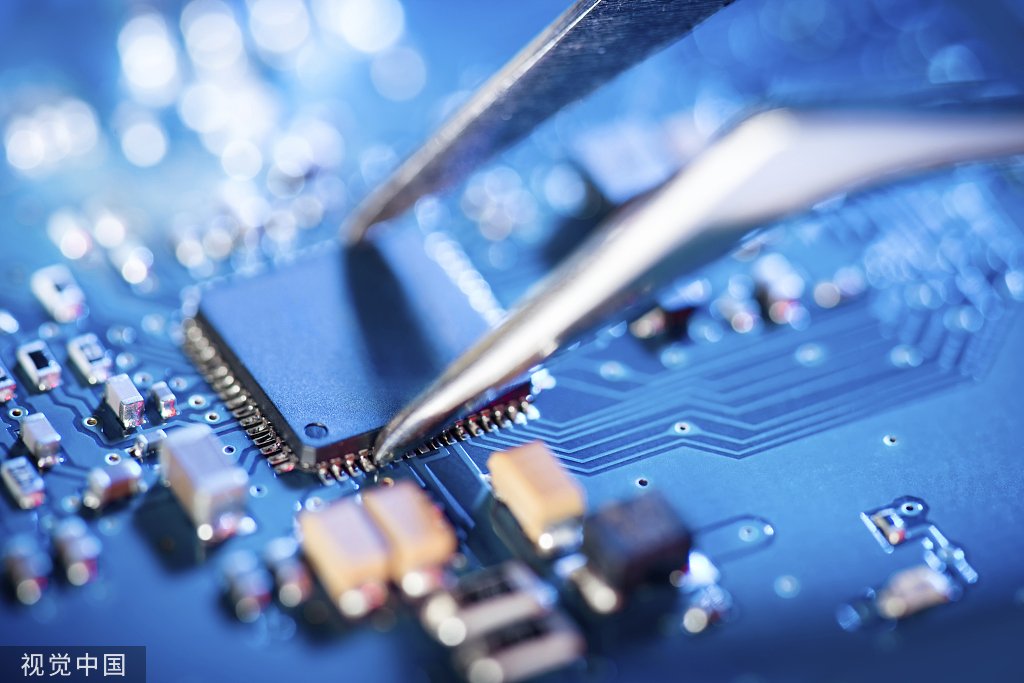
In the intricate world of electronics, Printed Circuit Boards (PCBs) serve as the backbone for a multitude of devices, enabling the complex interconnectivity required for modern technology. At the heart of PCB fabrication and longevity lies an essential process known as surface treatment. This process not only safeguards the board’s critical components but also ensures optimal functionality across its lifespan.
What is PCB Surface Treatment?
PCB surface treatment refers to the application of a protective layer over the board’s bare copper traces. This layer plays a pivotal role in preventing oxidation, which can degrade the copper over time and impair the board’s performance. Moreover, surface treatment enhances the solderability of the board, ensuring a reliable metal-to-metal connection between the board’s components and its copper traces. Positioned atop the copper layer, this protective coating acts as a shield, preserving the integrity and functionality of the PCB.
Surface treatments are not a one-size-fits-all solution; they vary significantly in composition, application process, and resultant properties. This diversity allows for tailored approaches to PCB manufacturing, where the choice of surface treatment can significantly influence the board’s quality, durability, and compatibility with specific electronic applications.
Types of PCB Surface Treatments
1. Hot Air Solder Leveling (HASL)
Hot Air Solder Leveling (HASL) stands as one of the most traditional methods of PCB surface treatment. It involves dipping the PCB into molten solder, which covers all exposed copper surfaces. Upon removal, high-pressure hot air (hence the name) evens out the solder deposit, removing excess and leaving a smooth, solderable surface behind. HASL comes in two varieties: leaded and lead-free, catering to different regulatory and environmental requirements. Despite its cost-effectiveness and reworkability, HASL can present challenges, such as uneven surface finishes and limitations with fine pitch components.
2. Immersion Tin (ImSn)
The Immersion Tin process applies a thin layer of tin over the copper surfaces using a chemical displacement reaction. This treatment is ideal for preserving the solderability of the copper, offering a flat surface that is highly compatible with various solder types. Although it boasts excellent surface flatness and moderate cost, ImSn can be sensitive to handling and has a relatively short shelf life, posing challenges for long-term storage and use.
3. Electroless Nickel Immersion Gold (ENIG)
ENIG employs a two-layer coating of nickel and gold over the copper traces, providing a robust barrier against oxidation while maintaining excellent solderability. This method is renowned for its flat surface, making it suitable for fine-pitch applications and offering a long shelf life. However, the complexity and cost of the ENIG process, alongside potential issues such as black pad syndrome, can deter its use in some contexts.
4. Organic Solderability Preservatives (OSP)
OSP involves applying a thin organic coating that protects the copper from oxidation without adding additional metals to the surface. This environmentally friendly option provides a flat surface ideal for soldering, especially in lead-free applications. Despite its advantages, OSP’s protective layer is not as durable as metallic options, limiting its shelf life and making it less suitable for through-hole technology (PTH).
5. Immersion Silver (ImAg)
Immersion Silver coats the PCB’s copper traces with a layer of silver, offering excellent conductivity and thermal stability. This surface treatment is a popular choice for its combination of good solderability, cost-effectiveness, and RoHS compliance. However, the silver surface is prone to tarnishing and requires careful handling and storage conditions to maintain its effectiveness.
6. Electroless Nickel Electroless Palladium Immersion Gold (ENEPIG)
ENEPIG adds a palladium layer between the nickel and gold layers, providing additional protection against corrosion and wear. This multi-layered approach yields an extremely flat and durable surface, suitable for multiple assembly cycles and demanding applications such as wire bonding. While ENEPIG offers comprehensive benefits, including lead-free compatibility and long shelf life, its cost and process complexity can be prohibitive for some projects.
7. Hard Gold Plating
Hard Gold Plating is specifically used for high-wear areas, such as edge connector contacts, where durability is paramount. This process involves electroplating a thick layer of gold over a nickel barrier, ensuring a hard, wear-resistant surface. While hard gold offers unmatched durability and a long shelf life, the high costs and additional processing requirements limit its use to specific applications where longevity and reliability are critical.

How to Choose the Right PCB Surface Treatment
Selecting the appropriate surface treatment for a PCB is a critical decision that impacts the board’s functionality, reliability, and cost. Key considerations include the required flatness and solderability of the surface, compatibility with wire bonding, storage conditions, the number of rework cycles the board might undergo, and compliance with RoHS regulations. For instance, ENIG and ENEPIG provide flat surfaces suitable for fine-pitch components, while HASL may be preferred for its cost-effectiveness and ease of rework in less demanding applications.
Each surface treatment comes with its unique set of advantages and drawbacks, making it essential to align the choice of treatment with the specific requirements of the PCB application. Factors such as the anticipated environmental conditions, assembly processes, and final product use should guide the selection process, ensuring that the chosen surface treatment optimally supports the PCB’s intended functionality.
Conclusion and A Look at Arisen Technology
In conclusion, understanding the nuances of PCB surface treatments is crucial for ensuring the durability, functionality, and compatibility of printed circuit boards with specific applications. As we’ve navigated through the complexities of various surface treatment options, it’s clear that the selection process is pivotal to achieving optimal outcomes in PCB manufacturing and assembly.
For those seeking expertise in PCB assembly and design services, Arisen Technology stands out as a prominent player in the field. Specializing in quick turn PCB prototypes and PCB design services, Arisen Technology provides comprehensive solutions tailored to meet the intricate demands of modern electronics manufacturing. Their commitment to quality and efficiency, coupled with advanced manufacturing capabilities, makes them a go-to option for both standard and complex PCB board projects. Whether you’re in need of fast PCB prototyping service or looking for a reliable partner for your microcontroller PCB design, Arisen Technology has the expertise and resources to bring your concepts to life.
Choosing the Right Wires for Breadboard Wiring: A Comprehensive Guide

Breadboards are a staple in electronic circuit building, offering flexibility and ease of use for both beginners and professionals. However, one of the most critical aspects of working with breadboards is selecting the right wires. The wires you choose can impact not only the functionality of your circuit but also its longevity and ease of…
How to Improve Heat Dissipation in PCB Design

Introduction As modern electronic devices become more complex and power-dense, heat dissipation has emerged as a critical factor that directly impacts device performance and reliability. Excessive junction temperatures in electronic systems can shorten the lifespan of components and lead to system failure. Thus, optimizing the PCB (Printed Circuit Board) design to improve heat dissipation is…
Manufacturing Process of Multilayer PCBs

Multilayer PCB manufacturing methods include the plated-through hole (PTH) and high-density interconnect (HDI) methods, both achieved by combining different processes to realize the circuit board structure. Currently, the most widely used method is the PTH method, which has been developed and refined over more than half a century. The PTH method is mature in terms…