The SATA interface is a connector between the hard drive and the host system, serving to transfer data between the hard drive cache and the host memory. Different hard drive interfaces determine the connection speed between the hard drive and the computer. In the entire system, the quality of the hard drive interface directly affects the speed of program operation and system performance.
Introduction to SATA Interface
SATA (Serial ATA) stands for Serial Advanced Technology Attachment, a new type of hard drive interface that is completely different from parallel ATA. The SATA interface uses an embedded clock signal, which has stronger error correction capabilities. The most significant difference compared to previous technologies is its ability to check transmission instructions (not just data). If errors are found, they are automatically corrected, significantly improving the reliability of data transmission. The SATA interface transmits 1 bit of data at a time, reducing the number of pins required and decreasing the number of connection cables, thus improving efficiency. SATA starts at a higher point and has more potential for development. SATA1.0 defines a data transfer rate of up to 150MB/sec, which is higher than the maximum 133MB/sec data transfer rate of the fastest parallel ATA (ATA/133). Currently, SATA2.0 has reached data transfer rates of up to 300MB/sec.
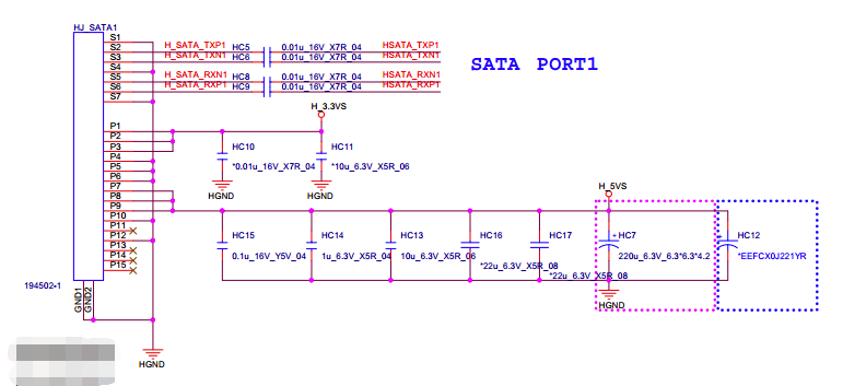
SATA Interface Pin Definition
– Ground (GND): The ground wire of the SATA interface is pin1, typically used to ground the device’s chassis and provide a low voltage for the interface.
– Data Positive (Data+): The positive data wire of the SATA interface is pin2, usually used to transmit the device’s data signal.
– Data Negative (Data-): The negative data wire of the SATA interface is pin3, typically used to return the device’s data signal.
It’s noteworthy that the pin definitions are the same among different SATA devices, making SATA connections between different devices possible. Additionally, the SATA interface supports hot swapping, allowing devices to be plugged and unplugged without powering down. Also, for 2.5-inch laptop serial hard drives, the +12V pin (i.e., the last three pins) is usually not connected directly to the power adapter or power strip.

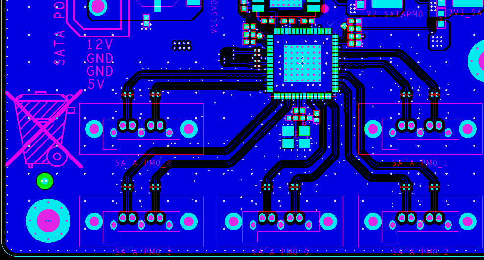
SATA Interface PCB Design
– Differential Impedance: The differential impedance of a SATA differential pair must be 100 ohms. If the impedance does not match, it can lead to unstable signal transmission and increase the error rate. Therefore, in PCB design, it’s necessary to ensure impedance matching of the differential pair through matching circuits or trace impedance design.
– Differential Pair Routing: The routing of differential pairs has very high requirements, including the length, width, spacing, and vias. In PCB design, differential pairs should be routed closely and at equal lengths, with spacing maintained at 6 to 10 times the trace width. Microstrip lines are recommended. If differential pairs must be routed on different layers, the lengths of traces on both sides of the vias must be identical. Additionally, it’s important to avoid placing differential pairs too close to other signals to prevent crosstalk.
EMI and Crosstalk
Due to the high transmission speeds of SATA interfaces, they can generate EMI (Electromagnetic Interference) and crosstalk. To reduce EMI and crosstalk, it’s essential to keep the routing distance of differential pairs under 150mil; the distance between differential pair routings should be 6 to 10 times (preferably 10 times) the height of the trace relative to the reference plane; avoid using test points on differential signals with Gb/s transmission speeds; and maintain a distance of at least 10 to 15 times the height of the trace relative to the reference plane for other signals on the same layer as the differential signal pairs.
Power and Ground
A stable power and ground supply is necessary for the SATA interface. In PCB design, a dedicated power layer and ground layer should be provided for the interface, ensuring the continuity of power and ground.
Test Points and Maintenance
To facilitate testing and maintenance, some test points, such as power test points, ground test points, and signal test points, should be designed at the interface. The position and number of test points should be designed according to actual needs without affecting the normal operation of the interface.
SATA Interface PCB Manufacturability Design
– Impedance Lines: In the manufacturing process, the tolerance for impedance lines is +/-10%, which is more precise than the +/-20% typically allowed for ordinary traces. Therefore, impedance line design should exceed the minimum manufacturing capability of ordinary lines.
– Pin Holes: The pin holes for SATA interface devices should be of appropriate size; too large, and the component may be loose, too small, and the component may not fit.
– Pads: The PCB pads for the SATA interface should be of appropriate size to facilitate soldering and maintenance.
– Testing: To ease testing and debugging, test points or test ports should be reserved on the PCB.
Enhancing PCB Design with Arisentec’s Expertise
In the realm of PCB manufacturing, Arisentec emerges as a leader, known for its excellence in PCB design services. Arisentec offers comprehensive solutions for microcontroller PCB design and electronic hardware design, catering to PCB board projects of various complexities and requirements.
Their commitment to quality and performance is paramount, especially for projects demanding high reliability, such as those involving SATA interfaces.
Arisentec’s approach to PCB design and manufacturing emphasizes precision and adaptability, catering to the intricate requirements of SATA-based storage solutions. Their services ensure that PCBs are not only functional but also optimized for performance, reflecting the importance of high-quality connections in modern computing environments.
Conclusion
By integrating Arisentec‘s capabilities in PCB design services into the framework of SATA interface development, the potential for enhanced system performance and reliability is significantly increased. This collaboration underscores the importance of selecting a skilled PCB manufacturer for projects that require meticulous attention to detail and high standards of quality.

Choosing the Right Wires for Breadboard Wiring: A Comprehensive Guide
Breadboards are a staple in electronic circuit building, offering flexibility and ease of use for both beginners and professionals. However, one of the most critical aspects of working with breadboards is selecting the right wires. The wires you choose can impact not only the functionality of your circuit but also its longevity and ease of…

How to Improve Heat Dissipation in PCB Design
Introduction As modern electronic devices become more complex and power-dense, heat dissipation has emerged as a critical factor that directly impacts device performance and reliability. Excessive junction temperatures in electronic systems can shorten the lifespan of components and lead to system failure. Thus, optimizing the PCB (Printed Circuit Board) design to improve heat dissipation is…

Manufacturing Process of Multilayer PCBs
Multilayer PCB manufacturing methods include the plated-through hole (PTH) and high-density interconnect (HDI) methods, both achieved by combining different processes to realize the circuit board structure. Currently, the most widely used method is the PTH method, which has been developed and refined over more than half a century. The PTH method is mature in terms…