High Speed Signal PCB Design
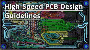
General high-speed signal PCB design processing principles are: (1) Level selection: When dealing with high-speed signals, the level with GND on both sides is preferred. (2) Priority
General high-speed signal PCB design processing principles are: (1) Level selection: When dealing with high-speed signals, the level with GND on both sides is preferred. (2) Priority