- 1. The Evolution of PCB Design Techniques
- 2. Material Innovations Shaping PCB Efficiency
- 3. Integration of CAD Tools with PCB Design
- 4. Precision Manufacturing Through Robotics
- 5. Adhering to Global Manufacturing Standards
- 6. Overcoming Modern Challenges: Miniaturization and Heat Dissipation
- 7. The Future of PCB Manufacturing: Smart Factories and IoT Integration
- Conclusion:
- Call to Action:
Introduction:
Printed Circuit Boards (PCBs) are the backbone of the electronics industry, supporting everything from simple gadgets to complex machinery. As technology progresses, the world of PCB manufacturing becomes increasingly complex and dynamic, necessitating a deep understanding and adaptability among professionals. For engineers and designers, staying at the forefront of PCB technologies is not just beneficial—it’s essential to maintaining relevance and competitiveness in this fast-paced industry.
The continuous evolution in materials, processes, and standards demands a proactive approach to learning and innovation. By examining these changes closely, professionals can anticipate trends and develop solutions that meet the high standards of today’s electronic products.
1. The Evolution of PCB Design Techniques
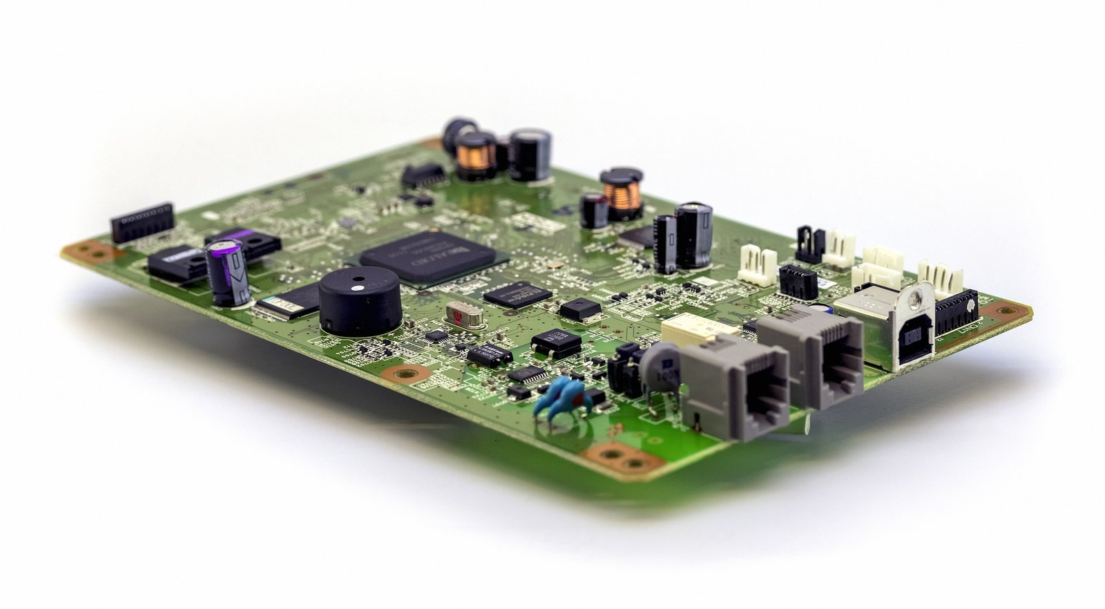
PCB design has transformed significantly over the decades, moving from basic single-layer boards to intricate multi-layered configurations that can support a vast array of electronic functions. This evolution has been driven by the need for more compact, efficient, and high-performing electronic devices. Today, designers must not only consider the electrical requirements of the PCB but also the mechanical and thermal aspects, which are crucial for ensuring reliability and functionality in diverse applications.
Case studies, such as those involving high-reliability sectors like aerospace or medical devices, reveal how sophisticated PCB designs can lead to breakthroughs in technology. For instance, multi-layer PCBs with high-density interconnects (HDIs) allow for faster signal transmission rates, which are critical in medical imaging devices. Such advancements underscore the importance of skilled PCB design in pushing the boundaries of what’s possible in electronics.
2. Material Innovations Shaping PCB Efficiency
In the realm of PCB manufacturing, the choice of substrate materials can profoundly impact the performance and longevity of the final product. Emerging materials such as high-frequency laminates and metal-core substrates are pivotal in meeting the demands for greater efficiency and durability. These materials help in managing thermal loads and reducing signal losses, which are critical factors in today’s high-speed electronic devices.
Environmental considerations are also shaping the selection of PCB materials. For instance, the industry is gradually shifting towards materials that are less harmful to the environment and promote sustainability. This shift not only helps companies adhere to stricter regulations but also appeals to a growing segment of environmentally conscious consumers. Innovations in biodegradable PCBs and the use of recycled materials are examples of how the industry is responding to environmental challenges.
3. Integration of CAD Tools with PCB Design
The integration of Computer-Aided Design (CAD) tools has revolutionized PCB design, making it more precise and efficient. Modern CAD software allows designers to create detailed models of PCBs that include every trace and component. These tools also support extensive simulation capabilities, enabling designers to test and tweak designs before they ever reach the fabrication stage, thereby reducing costly iterations.
Simulation plays a crucial role in anticipating design flaws and potential failure points under various operational conditions. By using these tools, engineers can ensure that the PCB will perform as expected in real-world conditions, which is essential for maintaining reliability and safety, particularly in critical applications like automotive or healthcare electronics.
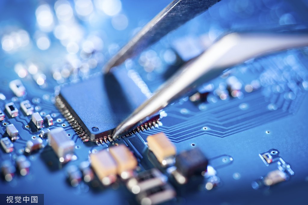
4. Precision Manufacturing Through Robotics
Robotics technology has made significant inroads into the PCB manufacturing process, particularly in the assembly phase. Automated robots are equipped with high-precision tools that can place components quickly and accurately, significantly reducing the possibility of human error and increasing production efficiency. This automation is crucial in industries where the volume of production and the need for precision are both high.
The adoption of robotic systems in PCB assembly not only speeds up the manufacturing process but also improves the consistency of the final products. For instance, at Arisentec, sophisticated robotic systems are employed to handle delicate operations that demand high accuracy, such as the placement of tiny, sensitive components on a PCB. This ensures high quality and reliability, which are paramount for maintaining client trust and satisfaction in competitive markets.
5. Adhering to Global Manufacturing Standards
Global standards are crucial in ensuring that PCBs are safe, reliable, and compatible across different devices and industries. Standards such as IPC, ISO, and UL define the criteria for design, materials, and testing that PCBs must meet to be considered compliant. These standards help manufacturers like Arisentec maintain a uniform level of quality and safety across all products, which is essential for global operations.
Compliance is not just about following rules—it’s about ensuring that every PCB that comes off the production line can perform its function effectively without causing harm or failure. It’s a crucial part of risk management and quality assurance in PCB manufacturing, protecting both the manufacturer and the end-users of the products.
6. Overcoming Modern Challenges: Miniaturization and Heat Dissipation
One of the most significant challenges in modern PCB design is miniaturization. As devices become smaller, the components and the PCBs themselves must shrink accordingly, which introduces a range of challenges from electrical interference to heat management. Effective strategies for miniaturization include using HDI technology and optimizing PCB layout service to maximize space without compromising the performance.
Heat dissipation is another critical challenge, especially as electronic devices become more powerful and compact. Innovations such as embedded cooling channels and heat sinks have become more prevalent in PCB designs to manage the increased thermal loads. At Arisentec, engineers utilize advanced thermal management techniques to ensure that PCBs can withstand the rigors of operation without overheating, thus extending the life of the product.
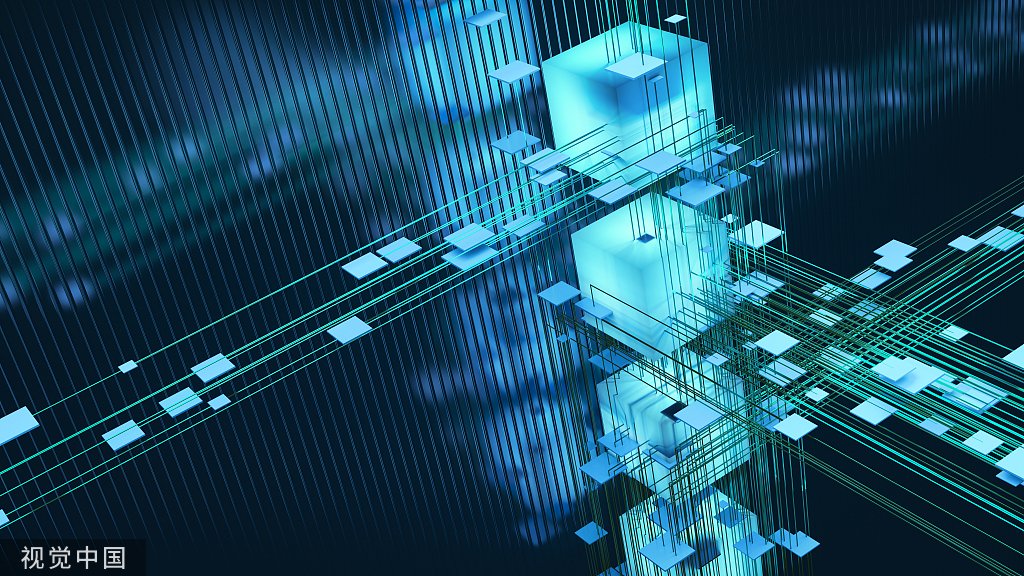
7. The Future of PCB Manufacturing: Smart Factories and IoT Integration
The future of PCB manufacturing lies in smart factories, where the Internet of Things (IoT) plays a pivotal role in streamlining production processes. IoT enables real-time monitoring of manufacturing operations, allowing for instant adjustments and improved decision-making. This integration leads to more efficient production cycles and minimal downtime, which are essential for meeting the growing demands of the electronics market.
Smart factories are set to revolutionize PCB manufacturing by enhancing the speed, flexibility, and customization of production. They enable manufacturers to quickly adapt to changes in demand or design specifications, providing a significant competitive advantage in a rapidly evolving industry.
Conclusion:
The landscape of PCB manufacturing is characterized by rapid technological advancements and increasing complexity. For designers and engineers, mastering these challenges is not just about keeping up with the latest trends—it’s about actively shaping the future of electronics. By embracing new materials, leveraging cutting-edge tools, and adhering to global standards, professionals can ensure that they remain at the forefront of this dynamic field.
Call to Action:
For those looking to deepen their knowledge and stay updated on the latest in PCB design and manufacturing, visiting Arisentec’s website offers valuable resources and insights. Engaging with the broader community through forums and webinars can also enhance understanding and foster innovation in PCB technologies.

Choosing the Right Wires for Breadboard Wiring: A Comprehensive Guide
Breadboards are a staple in electronic circuit building, offering flexibility and ease of use for both beginners and professionals. However, one of the most critical aspects of working with breadboards is selecting the right wires. The wires you choose can impact not only the functionality of your circuit but also its longevity and ease of…

How to Improve Heat Dissipation in PCB Design
Introduction As modern electronic devices become more complex and power-dense, heat dissipation has emerged as a critical factor that directly impacts device performance and reliability. Excessive junction temperatures in electronic systems can shorten the lifespan of components and lead to system failure. Thus, optimizing the PCB (Printed Circuit Board) design to improve heat dissipation is…

Manufacturing Process of Multilayer PCBs
Multilayer PCB manufacturing methods include the plated-through hole (PTH) and high-density interconnect (HDI) methods, both achieved by combining different processes to realize the circuit board structure. Currently, the most widely used method is the PTH method, which has been developed and refined over more than half a century. The PTH method is mature in terms…