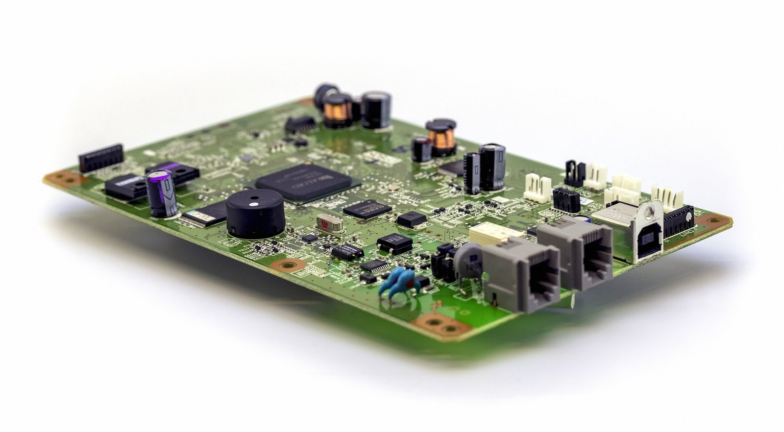
Testing a power supply PCB (Printed Circuit Board) is crucial to ensure the reliability and functionality of electronic devices. A meticulous testing process not only guarantees the efficiency of the power supply unit but also extends the lifespan of the connected components. At ArisenTec, we emphasize rigorous testing protocols to maintain the highest standards in PCB manufacturing. This guide provides a detailed overview of the methods and considerations involved in testing a power supply PCB, focusing on technical precision and adherence to industry standards.
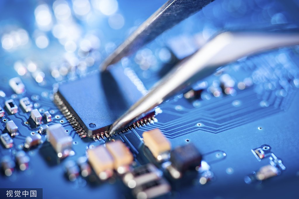
1. Visual Inspection
Before conducting electrical tests, a thorough visual inspection is essential. This step involves examining the PCB for any visible defects, such as:
· Soldering Issues: Look for cold joints, bridges, or voids in the solder. Poor soldering can lead to intermittent connections or complete failure of the power supply.
· Component Placement: Verify that all components are correctly placed according to the design specifications. Misaligned or incorrectly placed components can cause short circuits or improper functioning.
· Physical Damage: Check for any cracks, burns, or other signs of physical damage that could compromise the integrity of the PCB.
At ArisenTec, our pcba manufacturing process includes stringent visual inspections to catch these issues early, ensuring that only the highest quality products move forward in the production process.
2. Initial Power-Up Test
The initial power-up test is critical in assessing the PCB’s power supply functionality without putting the entire system at risk. Here’s how to conduct this test:
· Use a Current-Limited Power Supply: Connect the PCB to a current-limited power supply. Start with a low current limit to prevent damage in case of short circuits or other issues.
· Monitor Voltage Levels: Gradually increase the input voltage while monitoring the output voltage levels. Ensure that the outputs are within the expected range and stable.
· Check for Overheating: During the power-up, feel for any components that might be overheating. Overheating can indicate a fault or improper component selection.
3. Functional Testing
Functional testing ensures that the power supply PCB performs its intended operation under various conditions. This involves:
· Load Testing: Apply different loads to the power supply to verify that it can maintain the correct output voltage under varying conditions. Use resistive loads to simulate real-world operating conditions.
· Ripple and Noise Measurement: Use an oscilloscope to measure the ripple and noise on the output. Excessive ripple can indicate poor filtering or issues with the design of the power supply.
· Efficiency Testing: Measure the input and output power to calculate the efficiency of the power supply. An efficient design minimizes heat generation and energy consumption.
ArisenTec’s pcba factory is equipped with state-of-the-art tools to perform these functional tests, ensuring that every power supply PCB we produce operates efficiently and reliably.
4. Safety Testing
Ensuring that the power supply PCB adheres to safety standards is paramount. This includes:
· Isolation Testing: Verify the isolation between the input and output, especially in designs with high-voltage sections. Use a high-voltage insulation tester to ensure there is no leakage current that could pose a safety hazard.
· Overload and Short Circuit Protection: Test the power supply’s response to overload conditions and short circuits. The power supply should enter a protective shutdown mode or limit the output current to prevent damage.
5. Environmental Testing
Power supply PCBs must perform reliably under a variety of environmental conditions. Environmental testing includes:
· Thermal Cycling: Expose the PCB to temperature cycles that mimic operating conditions, including extremes of heat and cold. This tests the durability of the components and solder joints.
· Humidity Testing: Subject the PCB to high humidity conditions to ensure that it does not fail due to moisture ingress.
· Vibration and Shock Testing: Particularly important for automotive and industrial applications, this testing simulates the mechanical stress the PCB might encounter in its operating environment.
6. Documentation and Reporting
After completing the tests, it’s crucial to document the results meticulously. This documentation serves as a record of the PCB’s performance and is often required for regulatory compliance. The report should include:
· Test Conditions: A detailed description of the test setup, including the equipment used and the conditions under which the tests were conducted.
· Test Results: A comprehensive summary of the results, highlighting any deviations from expected performance and potential issues.
· Recommendations: Suggestions for improvements or further testing, if necessary.
Conclusion
Testing a power supply PCB is a multi-faceted process that requires attention to detail and a thorough understanding of electronic principles. By following the outlined steps—visual inspection, initial power-up, functional testing, safety testing, environmental testing, and proper documentation—you can ensure that the power supply PCB performs reliably and safely in its intended application. At ArisenTec, we are dedicated to delivering the highest quality PCBs through rigorous testing and adherence to industry best practices. This approach not only helps in identifying potential issues early in the development process but also contributes to the overall quality and longevity of the final product.
Choosing the Right Wires for Breadboard Wiring: A Comprehensive Guide

Breadboards are a staple in electronic circuit building, offering flexibility and ease of use for both beginners and professionals. However, one of the most critical aspects of working with breadboards is selecting the right wires. The wires you choose can impact not only the functionality of your circuit but also its longevity and ease of…
How to Improve Heat Dissipation in PCB Design

Introduction As modern electronic devices become more complex and power-dense, heat dissipation has emerged as a critical factor that directly impacts device performance and reliability. Excessive junction temperatures in electronic systems can shorten the lifespan of components and lead to system failure. Thus, optimizing the PCB (Printed Circuit Board) design to improve heat dissipation is…
Manufacturing Process of Multilayer PCBs

Multilayer PCB manufacturing methods include the plated-through hole (PTH) and high-density interconnect (HDI) methods, both achieved by combining different processes to realize the circuit board structure. Currently, the most widely used method is the PTH method, which has been developed and refined over more than half a century. The PTH method is mature in terms…