Introduction
As modern electronic devices become more complex and power-dense, heat dissipation has emerged as a critical factor that directly impacts device performance and reliability. Excessive junction temperatures in electronic systems can shorten the lifespan of components and lead to system failure. Thus, optimizing the PCB (Printed Circuit Board) design to improve heat dissipation is an essential challenge for every PCB designer. This article delves into several common methods for improving PCB heat dissipation, including increasing copper foil area, utilizing thermal vias, optimizing component placement, and selecting appropriate materials.
1. Increasing Copper Foil and Power Plane Area
Copper foil is the most commonly used thermal conductive material in PCBs, and increasing the area of the copper foil and power plane is an effective way to improve heat dissipation performance. By expanding the copper foil area, heat can be efficiently conducted away from heat-generating components to other parts of the PCB, reducing junction temperatures.

Effect of Copper Foil Area on Junction Temperature
Simulation data shows that as the copper foil area increases, heat dissipates more quickly, resulting in a significant reduction in junction temperature. For example, when both the top and bottom copper foil areas are 1.5 times the size of the component, the junction temperature decreases significantly.
In addition to improving heat dissipation, increasing the copper foil area also enhances the electrical performance of the PCB, allowing it to carry more current.
2. The Role of Thermal Vias
Thermal vias are an effective way to conduct heat between PCB layers. By incorporating thermal vias into the PCB, heat can be transferred from the top layer of heat-generating components to the bottom layers, increasing overall heat dissipation. Optimizing the number and layout of thermal vias can significantly improve the thermal performance of the PCB.

Comparison of Junction Temperature by Connection Type
Research shows that with a 6×6 thermal via array design, the junction temperature can be reduced by 4.8°C compared to designs without thermal vias. Additionally, thermal vias can minimize the temperature difference between the top and bottom surfaces of the PCB, enhancing overall thermal uniformity.
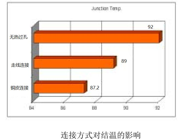
Comparison of Junction Temperature by Connection Type
3. Optimizing PCB Layout
The layout of components on a PCB directly impacts heat dissipation performance. A well-thought-out component placement can maximize airflow and minimize hotspots. Key strategies for optimizing PCB layout include:
Heat-sensitive component placement: Place heat-sensitive components in areas with better airflow to reduce their exposure to heat.
Power component arrangement: High-power components should be placed near the edge of the PCB to shorten heat conduction paths, and vertically, they should be positioned higher to minimize the impact on other components.
Zoning design: Group components based on heat generation levels, ensuring that high-power and low-power components are separated to prevent excessive heat concentration.

By studying airflow paths, designers can ensure that cooling air effectively passes through the PCB to maximize heat dissipation. Ensuring no large voids in the PCB helps prevent air short circuits, another important consideration in layout design.
4. Material Selection for Heat Dissipation
In addition to layout design, material selection plays a crucial role in PCB heat dissipation. High thermal conductivity materials, such as TIF thermal silicone pads, can enhance overall heat dissipation without adding PCB thickness.

Heat Source DIE and TIF Thermal Silicone Pad
These thermal materials fill the gaps between components and the PCB, reducing interface thermal resistance and allowing heat to transfer more quickly to the heat sink.
5. Integrated Heat Dissipation Solutions
To further improve heat dissipation performance, multiple heat dissipation techniques can be combined. By using copper foils, thermal vias, optimized layouts, and thermal materials together, designers can significantly enhance heat dissipation, reduce junction temperatures, and improve system reliability.
Conclusion
By increasing the copper foil area, using thermal vias, optimizing PCB layout, and selecting high thermal conductivity materials, designers can effectively improve the heat dissipation performance of PCBs. These measures not only reduce component junction temperatures but also extend the lifespan of devices. As the power density of electronic products continues to rise, the importance of PCB thermal design will become increasingly evident. By implementing these optimization techniques, engineers can ensure their products maintain reliable performance even in high-temperature environments.
The picture is reproduced from wechat public channel: PCB circuit board home, for more information, please click https://arisentecpcb.com/

Choosing the Right Wires for Breadboard Wiring: A Comprehensive Guide
Breadboards are a staple in electronic circuit building, offering flexibility and ease of use for both beginners and professionals. However, one of the most critical aspects of working with breadboards is selecting the right wires. The wires you choose can impact not only the functionality of your circuit but also its longevity and ease of…

How to Improve Heat Dissipation in PCB Design
Introduction As modern electronic devices become more complex and power-dense, heat dissipation has emerged as a critical factor that directly impacts device performance and reliability. Excessive junction temperatures in electronic systems can shorten the lifespan of components and lead to system failure. Thus, optimizing the PCB (Printed Circuit Board) design to improve heat dissipation is…

Manufacturing Process of Multilayer PCBs
Multilayer PCB manufacturing methods include the plated-through hole (PTH) and high-density interconnect (HDI) methods, both achieved by combining different processes to realize the circuit board structure. Currently, the most widely used method is the PTH method, which has been developed and refined over more than half a century. The PTH method is mature in terms…