Understanding PCB Ballasts
PCB ballasts are electrical components used in lighting fixtures, particularly in fluorescent lights, to regulate current and provide the necessary voltage to start the lamp. In this context, “PCB” refers to polychlorinated biphenyls, a group of man-made organic chemicals. Due to their excellent insulating properties, PCB ballasts were widely used until they were banned in the late 1970s. However, because of their toxicity and environmental impact, identifying and properly handling PCB ballasts is crucial for safety and regulatory compliance.
Key Characteristics of PCB Ballasts
1. Manufacturing Date: The first step in identifying a PCB ballast is to check the date of manufacture. PCB ballasts were commonly used in ballasts produced before 1979, particularly in the United States. If the ballast was manufactured after this date, it is likely to be non-PCB, although verification is still recommended.
2. Labeling: Many manufacturers labeled their ballasts with the words “Contains PCBs.” However, this labeling is not always present. Conversely, newer ballasts might be labeled “No PCBs,” indicating they are free from these hazardous chemicals.
3. Manufacturer’s Information: Check the brand and model number of the ballast. This information can often be cross-referenced with manufacturer databases or regulatory agencies to confirm whether the ballast contains PCBs.
4. Physical Inspection: Older ballasts containing PCBs may show signs of wear, such as leaking oil or tar, which could be due to the breakdown of PCB compounds. If any substance is leaking from the ballast, it should be treated as hazardous and handled with extreme caution.
5. Regulatory Resources: Various environmental protection agencies provide guidelines and databases to help identify PCB-containing ballasts. For instance, the U.S. Environmental Protection Agency (EPA) offers resources that can determine whether a ballast contains PCBs based on its make, model, and date of manufacture.
Safety Precautions
When dealing with PCB ballasts, safety is paramount. If a ballast is suspected to contain PCBs, it should be handled and disposed of according to local and federal regulations. This often involves specific procedures for containment, transport, and disposal to prevent environmental contamination and human exposure. Always consult environmental safety experts or refer to official guidelines when dealing with PCB ballasts.
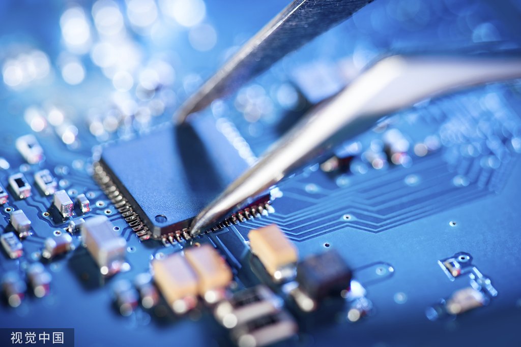
Companies like ArisenTec, a leading PCBA manufacturer, prioritize adherence to environmental and safety regulations during the design and manufacturing process. Particularly in PCBA manufacturing, identifying and safely handling components that may contain PCBs is crucial for producing high-quality, environmentally compliant circuit boards.
By partnering with a reliable PCBA manufacturer like ArisenTec, businesses can ensure that their electronic products not only perform optimally but also meet stringent environmental standards. This commitment to professionalism and attention to detail sets ArisenTec apart as a trusted partner in the industry.
When choosing a PCB manufacturer, understanding how they manage hazardous materials like PCB ballasts is essential. This not only affects product quality but also the health and safety of the environment and workers. By relying on ArisenTec’s expertise and experience, businesses can be confident that their products will meet the highest environmental and safety standards.

Choosing the Right Wires for Breadboard Wiring: A Comprehensive Guide
Breadboards are a staple in electronic circuit building, offering flexibility and ease of use for both beginners and professionals. However, one of the most critical aspects of working with breadboards is selecting the right wires. The wires you choose can impact not only the functionality of your circuit but also its longevity and ease of…

How to Improve Heat Dissipation in PCB Design
Introduction As modern electronic devices become more complex and power-dense, heat dissipation has emerged as a critical factor that directly impacts device performance and reliability. Excessive junction temperatures in electronic systems can shorten the lifespan of components and lead to system failure. Thus, optimizing the PCB (Printed Circuit Board) design to improve heat dissipation is…

Manufacturing Process of Multilayer PCBs
Multilayer PCB manufacturing methods include the plated-through hole (PTH) and high-density interconnect (HDI) methods, both achieved by combining different processes to realize the circuit board structure. Currently, the most widely used method is the PTH method, which has been developed and refined over more than half a century. The PTH method is mature in terms…