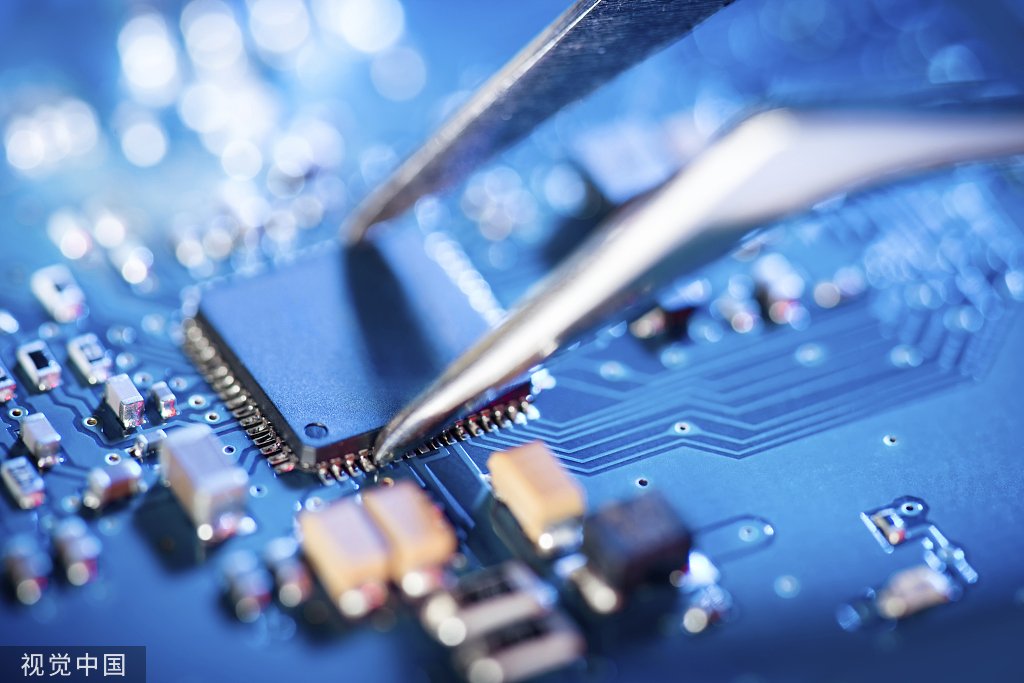
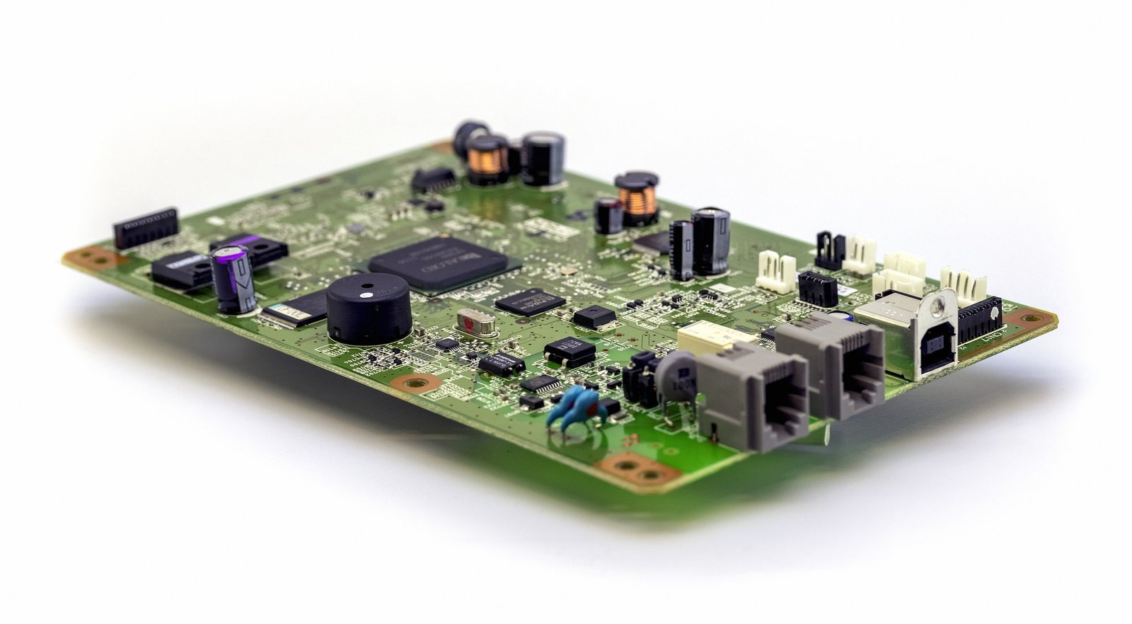
Printed Circuit Board (PCB) design is a critical aspect of electronics manufacturing, playing a vital role in the functionality, reliability, and overall performance of electronic devices. As the demand for sophisticated electronics grows, so does the need for skilled PCB designers. This guide outlines the steps and skills required to become a successful PCB designer, with an emphasis on industry standards, technical competencies, and career development.
1. Understanding the Role of a PCB Designer
A PCB designer is responsible for creating the layout of the circuit boards that connect electronic components in a device. This involves translating schematics into a physical design that can be manufactured efficiently and meets all technical specifications. PCB designers work closely with engineers to ensure that the design meets electrical performance, mechanical constraints, and manufacturability requirements. They must be proficient in specialized software and have a deep understanding of materials, signal integrity, and thermal management.
2. Educational Background and Skills Development
To become a PCB designer, a strong foundation in electronics and electrical engineering is essential. Most PCB designers hold a degree in electrical engineering, electronics engineering, or a related field. Coursework in circuit theory, digital systems, and materials science is particularly beneficial.
In addition to formal education, aspiring PCB designers should focus on developing the following skills:
· Proficiency in PCB Design Software: Familiarity with industry-standard design tools such as Altium Designer, Allegro, or OrCAD is crucial. These tools are used to create the schematics, layout, and documentation required for PCB manufacturing.
· Understanding of Industry Standards: Knowledge of IPC standards, which govern PCB design and manufacturing, is vital for ensuring designs meet industry requirements. Designers should also be aware of safety regulations and environmental considerations.
· Attention to Detail: PCB design requires meticulous attention to detail, as even minor errors can lead to costly manufacturing defects or performance issues.
· Problem-Solving Skills: Designers must be able to troubleshoot and resolve issues related to signal integrity, component placement, and thermal management during the design process.
3. Gaining Practical Experience
Practical experience is key to becoming a proficient PCB designer. This can be gained through internships, co-op programs, or entry-level positions in electronics manufacturing companies. Working on real-world projects allows designers to apply their theoretical knowledge and gain insight into the challenges of PCB design and pcba manufacturing.
· Prototyping and Testing: Participating in pcb prototyping services provides hands-on experience in creating and testing designs, allowing designers to refine their skills and understand the impact of design choices on manufacturability and performance.
· Collaboration with Engineers: PCB designers often work as part of a multidisciplinary team, collaborating with electrical engineers, mechanical engineers, and manufacturing specialists. This teamwork is crucial for ensuring that the PCB design integrates seamlessly with other components of the product.
4. Advanced Training and Specialization
As PCB designers gain experience, they may choose to specialize in areas such as high-speed digital design, RF design, or flexible PCB design. Specialization often requires additional training and certification.
· Advanced Certifications: Earning certifications from organizations such as IPC can demonstrate a designer’s expertise in specific areas of PCB design and can enhance career prospects. For example, an IPC Certified Interconnect Designer (CID) certification is highly regarded in the industry.
· Continuous Learning: The field of PCB design is constantly evolving, with new technologies and materials emerging regularly. Staying up-to-date with the latest advancements through courses, seminars, and industry publications is essential for maintaining a competitive edge.
5. Building a Professional Portfolio
A strong portfolio showcasing your PCB design projects is crucial for advancing your career. This portfolio should include a variety of projects that demonstrate your ability to handle different design challenges, such as flex pcb stiffener integration, multi-layer board design, and turnkey pcb assembly.
· Documentation and Presentation: Include detailed documentation of each project, highlighting your role in the design process, the tools you used, and the challenges you overcame. High-quality visual presentations of your designs can also make a significant impact.
· Networking and Professional Associations: Joining professional associations, such as the IPC Designers Council, and attending industry conferences can provide valuable networking opportunities and keep you informed about industry trends.
6. Career Opportunities and Advancement
PCB designers have a wide range of career opportunities in various industries, including consumer electronics, automotive, aerospace, and telecommunications. As designers gain experience and build their portfolios, they can advance to roles such as senior PCB designer, design engineer, or even move into management positions within the pcba factory.
· Freelancing and Consulting: Experienced PCB designers may choose to work as freelancers or consultants, offering their expertise to multiple clients across different industries. This path offers greater flexibility and the potential for higher earnings.
· Innovation and Entrepreneurship: For those with a strong entrepreneurial spirit, starting a PCB design consultancy or pcba manufacturing company could be a viable path, allowing you to apply your expertise to innovate and lead in the industry.
7. Conclusion
Becoming a PCB designer requires a combination of technical knowledge, practical experience, and continuous learning. By focusing on developing a strong educational foundation, gaining hands-on experience, and building a professional portfolio, aspiring designers can position themselves for success in this dynamic and rewarding field. As the demand for advanced electronics continues to grow, skilled PCB designers will remain essential to the development of cutting-edge technologies.
For more information about PCB design and manufacturing, visit ArisenTec to explore our services and expertise in delivering high-quality, custom-designed PCBs.

Choosing the Right Wires for Breadboard Wiring: A Comprehensive Guide
Breadboards are a staple in electronic circuit building, offering flexibility and ease of use for both beginners and professionals. However, one of the most critical aspects of working with breadboards is selecting the right wires. The wires you choose can impact not only the functionality of your circuit but also its longevity and ease of…

How to Improve Heat Dissipation in PCB Design
Introduction As modern electronic devices become more complex and power-dense, heat dissipation has emerged as a critical factor that directly impacts device performance and reliability. Excessive junction temperatures in electronic systems can shorten the lifespan of components and lead to system failure. Thus, optimizing the PCB (Printed Circuit Board) design to improve heat dissipation is…

Manufacturing Process of Multilayer PCBs
Multilayer PCB manufacturing methods include the plated-through hole (PTH) and high-density interconnect (HDI) methods, both achieved by combining different processes to realize the circuit board structure. Currently, the most widely used method is the PTH method, which has been developed and refined over more than half a century. The PTH method is mature in terms…