- PCB – The Foundation of Electronic Devices
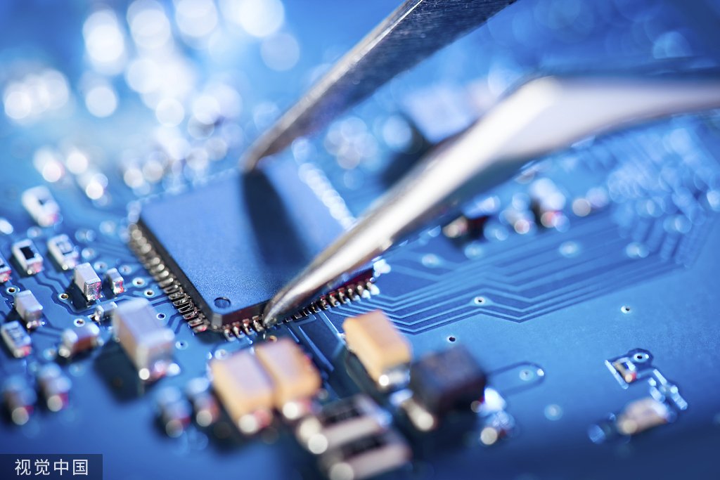
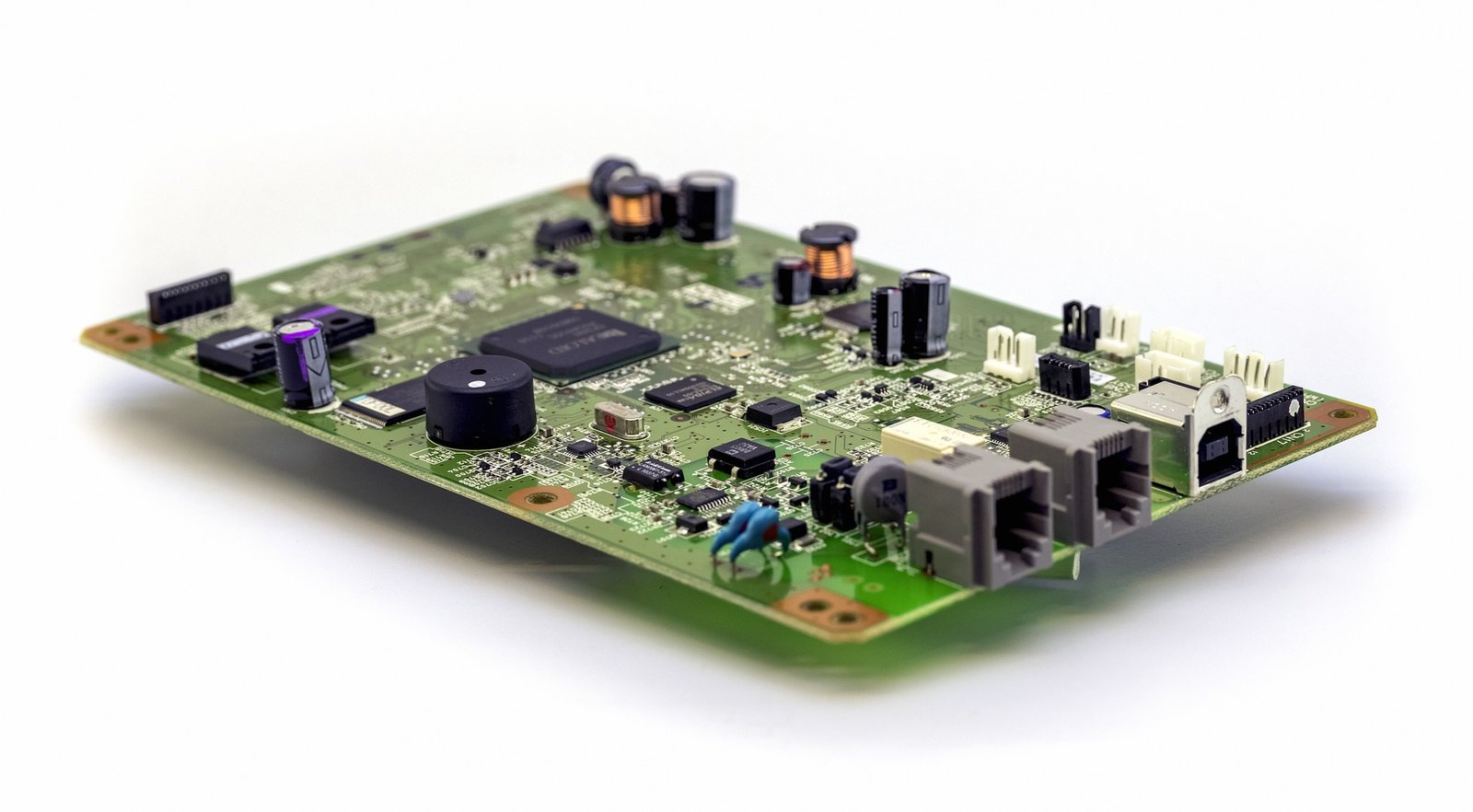
- PCBA – The Assembly of Electronic Components
- PCB and PCBA Relationship
- Differences between PCB and PCBA
- Understanding the PCB Manufacturing Process
- Understanding the PCBA Manufacturing Process
- Benefits of Using PCB
- Benefits of Using PCBA
- Challenges and Considerations in PCB Assembly
- Quality Control in PCB Manufacturing
- Future Trends in PCB and PCBA Technology
Do you know the importance of Printed Circuit Board (PCB) and Printed Circuit Board Assembly (PCBA)? These are two interchangeable terms that are basic part of the manufacturing and assembly of electronic devices. In this article we will explore what is key role of PCB and PCBA in the production process?
PCB – The Foundation of Electronic Devices
A PCB is basically a conductive pathway consisted flat board that made up of material, such as fiberglass. The pathway that called traces is a gateway for electronic circuit. The PCB provide basic framework for mounting electronic components and facilitating the flow of electrical signals between them.
Based on the required circuit or application there are different type of PCB in different shapes, sizes, and layers. There is computer-aided design (CAD) software that use to design PCB according to connection requirement such as single-sided, double-sided, or multi-layered.
Once the CAD completes the design process the next step manufacturing process involves techniques like etching, drilling, and soldering.
PCBA – The Assembly of Electronic Components
As PCB is a computerized print on the other hand PCBA is assembling of electronic component circuit on that design to complete the circuit. For this purpose you need to have basic tools such as pick-and-place machines and reflow ovens, to accurately position and attach the electronic components onto the PCB. The assembling of PCBA on PCB involve different pcba manufacturing steps, such as

* Component placement
* Soldering
* Inspection and testing
There are two common technology named Surface Mount Technology (SMT) and Through-Hole Technology (THT) use for PCBA. SMT use to mount components directly on the PCB while for larger components insertion through pre-drilled holes and soldering THT is one of the best method.
PCB and PCBA Relationship
Both PCB and PCBA are integral parts of the electronics manufacturing process. Where the PCB provide a frame work design at the same time PCBA adds the components that bring the circuit to life.
The success of the electronic application or device based on both PCB and PCBA. A well-designed and properly manufactured PCB ensures success of the circuit similarly a poorly designed or faulty PCB can lead to assembly issues that lead to malfunctioning.
Differences between PCB and PCBA
Although PCB and PCBA use interchangeably but both are different terms. PCB refers to the CAD software based design on circuit board while PCBA stands for printed circuit board assembly. Here are the main distinctions between PCB and PCBA:
Component Placement:
One of the main differences between PCB and PCBA is the stage of component placement. PCBs are bare boards that do not have any electronic components attached to them. They serve as the foundation for the circuitry, providing the necessary paths for electrical connections. On the other hand, PCBA involves the assembly process where electronic components, such as resistors, capacitors, and integrated circuits, are mounted onto the PCB.
Manufacturing Process
The PCB is a printed circuit board design on fiberglass or ceramic that is according to the desired circuit pattern. While PCBA is assembling of electronic components on the pre designed PCB to make the circuit functional. This assembly process may be manual or automated, depending on the complexity and volume of the production.
Functionality
PCB provide base platform and structure for the electronic components. PCB can bot perform any function on their own. While PCBA is a functional unit by the use of electronic circuit. Once the electronic components are mounted on the PCB and soldered into place, the assembly becomes a complete and functional electronic device.
Testing and Quality Control
Due to their basic manufacturing difference the testing and quality control procedures are different. For PCBs the testing involves checks for continuity, insulation resistance, and impedance. On the other hand for PCBA reliability the testing includes in-circuit testing (ICT), and burn-in testing.
Application
PCBs are widely used in various industries and applications as the backbone of electronic devices. They are utilized in computers, smartphones, automotive systems, medical devices, and many other electronic products. PCBA, on the other hand, is specific to a particular product or device. It represents the final stage of manufacturing where all the necessary components are assembled onto the PCB to create a functional electronic system.
In this way both PCB and PCBA are key part of any electronic circuit. Where PCB provide foundation for electronic circuit the PCBA PCBA is the complete assembly of components on that design frame.
Understanding the PCB Manufacturing Process
The PCB manufacturing process is a complex and intricate series of steps that transform raw materials into functional printed circuit boards. Understanding this process is crucial for anyone involved in the PCB industry, as it can help in making informed decisions regarding the design, production, and quality control of PCBs.
1. Designing the PCB: The process begins with designing the PCB layout using computer-aided design (CAD) software. This involves placing components and tracing the connections between them.
2. Generating Gerber files: After designing the layout, the CAD software generates Gerber files that contain all the necessary data for the manufacturing process. These files serve as a blueprint for the production of the PCB.
3. Material selection: The next step involves selecting the appropriate materials for the PCB. This includes choosing the type of substrate, copper weight, and solder mask. The choice of materials depends on various factors such as the desired board thickness, electrical properties, and cost considerations.
4. Print and etch process: In this step, a layer of copper is applied to the substrate material, typically through a process called electroplating. The excess copper is then etched away, leaving behind the desired circuit pattern.
5. Drilling: Holes are drilled into the PCB to accommodate components and allow the traces to interconnect layers. The drilling process requires precision as even a minor misalignment can cause issues during assembly.
6. Plating: After drilling, the holes are plated with a thin layer of copper to create a conductive connection between the different layers of the PCB. This process is known as plating or electroless copper deposition.
7. Solder mask application: A solder mask is applied to the PCB to protect the copper traces from oxidation and to provide insulation between them. The solder mask also helps in ensuring proper soldering during component assembly.
8. Silkscreen printing: Information such as component names, reference designators, and logos are printed onto the PCB using a special ink called solder paste. This allows for easier identification and assembly of components.
9. Component assembly: Once the PCB is ready, components like resistors, capacitors, and integrated circuits are placed on the board using automated machinery. The components are then soldered onto the board to establish electrical connections.
10. Testing and inspection: Quality control is a critical part of the PCB manufacturing process. PCBs undergo various tests, such as electrical testing, functionality testing, and visual inspection, to ensure they meet the required specifications and standards.
11. Final finishing and packaging: After successful testing, the PCBs are cleaned, and any remaining solder mask or debris is removed. The boards are then coated with a protective finish and packaged before they are ready for shipment.
Understanding the PCB manufacturing process from start to finish is essential for manufacturers, engineers, and designers alike. It not only help in better decision-making but allow to improve quality for reliable and high-performing PCBs.
Understanding the PCBA Manufacturing Process
Understanding the PCBA manufacturing process is crucial for anyone involved in the design, development, or production of electronic devices. There are some of the steps that involve in PCBA manufacturing process.
1. Component Sourcing and Procurement
It is essential to ensure the quality and authenticity of the components to avoid any potential issues during the manufacturing process. This step in the PCBA manufacturing process consists on identification of required components, selecting reliable suppliers, and procuring the components needed for the assembly.
2. PCB Fabrication
High precision and attention to detail are crucial during this stage to ensure the proper functioning and reliability of the final product. It involves transferring the PCB design onto the board, and etching the circuitry with the help of drilling holes, applying solder mask, and adding silkscreen markings.
3. Component Placement
Once the PCB is ready now with the help of automated machinery or manual labor components are carefully placed onto the designated pads on the PCB. The accuracy and alignment of the components are crucial to ensure proper electrical connections and functionality.
4. Soldering
After the components are placed, the next stage is soldering. Soldering is the process of permanently attaching the components to the PCB that you can do with a metal alloy with a low melting point.
For this purpose professional use wave soldering, reflow soldering, or manual soldering techniques. The solder creates electrical connections between the components and the PCB, ensuring proper signal flow and stability.
5. Inspection and Testing
Once the soldering is complete now need to identify any manufacturing defects, component failures, or soldering issues. You can do inspection with visual inspection, automated optical inspection (AOI), or X-ray inspection. Functional testing is also performed to ensure the proper operation of the assembled electronic device.
6. Quality Assurance and Packaging
After passing the inspection and testing stages, the assembled PCBs undergo to meet quality standards and specifications. Once approved, the PCBs are packaged according to the customer’s requirements. Packaging may include anti-static bags, trays, or boxes, depending on the nature of the electronic device and its intended use.
By understanding the PCBA manufacturing process and following these steps diligently, manufacturers can ensure the production of reliable and functional electronic products that meet customer expectations.
Benefits of Using PCB
PCB is key part of the electronic devices and applications. There are several benefits of PCB. Some of the common are
1. Compact and Space-Efficient Design
By elimination of extensive wiring and bulky connections PCB is compact and space-efficient design. It allows making light weight and small size product that is efficient for users.
2. Reliable and Consistent Performance
With the use of copper tracks there is low level of resistance that ensures proper signal flow. It provides electromagnetic interference (EMI) that lowers the signal disruptions.
3. Increased Durability and Stability
PCB due to rigid structure provides support against mechanical stress, vibrations, and impacts. This durability makes it ideal for aerospace, automotive, and industrial systems.
4. Ease of Repairs and Maintenance
With easy and well-designed layout PCB ease in identification and elimination of faulty component. Now the repairing process become more simple and convenient.
5. Cost-Effective Manufacturing
PCB is computerized print design that have low chances of defective products. It also reduce labor cost and ensure faster production. In this way it saves both time and money.
6. Design Flexibility and Customization
This digital print layout eases in customization to meet specific requirements of client. It opens the door of innovation to create unique features and functionalities for manufacturers.
7. Environmental Benefits
The whole manufacturing involves waste free process that is responsible for sustainability of the manufacturing process. It is evergreen process due to minimum use of wires and connectors, and ability to recycle materials.
In this way PCBs in electronic devices offers a wide range of benefits, including compact design, reliable performance, durability, ease of repairs, cost-effectiveness, design flexibility, and environmental sustainability.
Benefits of Using PCBA
PCB is linked with PCBA for functionality of devices. The benefits that linked with PCBA (Printed Circuit Board Assembly) are
Using PCBA (Printed Circuit Board Assembly) offers several benefits over using just a PCB (Printed Circuit Board). These benefits make PCBA a popular choice for manufacturers in various industries. Here are some of the key advantages of using PCBA:
1. Cost-effectiveness: PCBA minimize the labor cost and manual inspection. Due to elimination of manual insulation it is low cost approach.
2. Enhanced functionality: PCBA allows for the integration of complex electronic components onto the PCB, including microcontrollers, sensors, and other active and passive devices.
3. Increased reliability: In PCBA the level of accuracy is high due to use of surface mount technology (SMT) or through-hole technology (THT). There is minimal chance of loose connections or faulty soldering.
4. Faster time to market: With use of high end technology and computerize system the assembling process speed up. This automates process, accelerate the product development cycle.
5. Quality assurance: There is automated computerize inspection and testing of final product. That ensures prompt corrections and minimizing the risk of fault.
6. Scalability: PCBA offers scalability for production volumes that is effective for businesses during fluctuating market demands or seasonal variations in sales.
These advantages make PCBA an attractive choice for manufacturers looking to optimize their production processes efficiently.
Challenges and Considerations in PCB Assembly
Due complexity of PCB assemblers process you need to focus on key steps to meet challenges. There are several challenges and considerations that must be taken into account during the PCB assembly process.
1. Design for Manufacturability (DFM): First of all you need to assure that the design of the PCB is suitable for the manufacturing process. Design for Manufacturability (DFM) analysis helps identify potential issues early in the process, reducing the risk of costly rework or assembly failures.
2. Component Sourcing: The choice of components can have a significant impact on the overall quality and reliability of the final product. It’s necessary to choose right component by focusing on factors such as component availability, cost, reliability, and lead times.
3. Quality Control and Testing: Ensuring the quality and reliability of the assembled PCBs is necessary to reduce chances of fault. Manufacturers often employ automated testing equipment to evaluate the functionality of the PCBs and ensure they meet the specified standards.
4. Soldering Techniques: Proper soldering techniques whether it’s through-hole soldering or surface mount technology (SMT), are essential for PCB. Both techniques have their advantages and challenges, and manufacturers need to select the most suitable option based on factors such as component density, board size, and solder joint reliability.
5. Thermal Management: Designing and implementing appropriate heat dissipation techniques, such as heat sinks or thermal pads, are essential to maintain optimal operating temperatures and prevent thermal stress.
6. Environmental Considerations: There are environmental factors such as temperature, humidity, vibration, and electrical noise that impact the performance and reliability of the final product. Keep in mind to choose component that can withstand the intended operating conditions to ensure long-term stability and reliability.
Quality Control in PCB Manufacturing
In the world of electronics manufacturing, quality control is paramount. You must need to focus on quality over quantity for PCB. Here are some key aspects of quality control in PCB manufacturing:
1. Design Verification
Prior to PCB fabrication, must ensure that the design meets all the necessary requirements. This step helps in identifying potential issues and making necessary modifications before the manufacturing process begins.
2. Material Inspection
Any deviations or defects can lead to performance issues or failure of the PCB. A basic part of quality control is the inspection of materials. For this focus on key things such as copper-clad laminates, solder mask, and solder paste, to ensure they meet the required specifications.
3. Electrical Testing
Electrical testing is a crucial quality control step that helps identify any potential faults or defects that may affect the performance of the PCB.
4. Fabrication Process Controls
To ensure the quality in fabrication process keep eye on controlling the etching, drilling, plating, and solder mask application processes. Regular inspections and measurements are conducted to ensure that the dimensions, tolerances, and quality of each PCB layer are within acceptable limits.
5. Quality Management System
A comprehensive quality management system (QMS) is essential to ensures that all quality control activities are adequately documented, monitored, and reviewed according to set desired quality objectives.
6. Visual Inspection
Visual inspection is another vital aspect of quality control ensures that the PCBs meet the required cosmetic standards and eliminates any visible issues that may affect performance or reliability.
Future Trends in PCB and PCBA Technology
In the ever evolving landscape of technology the field of PCB (Printed Circuit Board) and PCBA (Printed Circuit Board Assembly). Here are some of the prominent future trends to watch out for:
1. Miniaturization and Increased Density:
One of the most evident trends in PCB and PCBA technology is the ongoing drive towards miniaturization and increased density.
With advancements in semiconductor technology and the demand for smaller, more compact electronic devices, PCBs are being designed to accommodate more components in a smaller space. This trend is particularly significant in industries such as medical, aerospace, and wearable devices.
2. High-Speed PCBs:
The growing need for faster and more efficient electronic devices has led to the development of high-speed PCBs. High-speed PCBs are crucial for applications such as telecommunications, data centers, and consumer electronics.
3. Flexible and Rigid-Flex PCBs:
Flexible and rigid-flex PCBs are gaining popularity due to their unique design capabilities. Flexible PCBs are extremely thin and lightweight that is ideal choice due to flexibility. Rigid-flex PCBs combine both flexible and rigid materials that make it appropriate for more complex three-dimensional designs. These types of PCBs are increasingly used in industries such as automotive, aerospace, and medical devices.
4. Increased Integration of IoT and Smart Devices:
As the Internet of Things (IoT) continues to grow, the integration of PCBs and PCBA technology with smart devices is becoming more prevalent. The future will witness a proliferation of IoT-enabled devices, creating a demand for advanced PCB and PCBA technology to handle the increasing complexity and connectivity requirements.
5. Advanced Materials and Manufacturing Techniques:
To meet the evolving demands of the industry, there is a rise in the use of advanced materials and manufacturing techniques.
New materials with enhanced thermal conductivity, and innovative manufacturing techniques such as 3D printing and additive manufacturing are making their way into the PCB and PCBA industry, providing more flexibility and design possibilities.
6. Integration of Artificial Intelligence and Machine Learning:
The integration of artificial intelligence (AI) and machine learning (ML) in PCB and PCBA technology is on the horizon. AI and ML algorithms play a crucial role in increasing efficiency, reducing costs, and advancing the capabilities of PCB and PCBA technology.
In this way the future of PCB and PCBA technology is bright with innovation and trends to watch out for. Staying up-to-date with these trends is essential to remain part of this innovative ever evolving market race for businesses and professionals.

Choosing the Right Wires for Breadboard Wiring: A Comprehensive Guide
Breadboards are a staple in electronic circuit building, offering flexibility and ease of use for both beginners and professionals. However, one of the most critical aspects of working with breadboards is selecting the right wires. The wires you choose can impact not only the functionality of your circuit but also its longevity and ease of…

How to Improve Heat Dissipation in PCB Design
Introduction As modern electronic devices become more complex and power-dense, heat dissipation has emerged as a critical factor that directly impacts device performance and reliability. Excessive junction temperatures in electronic systems can shorten the lifespan of components and lead to system failure. Thus, optimizing the PCB (Printed Circuit Board) design to improve heat dissipation is…

Manufacturing Process of Multilayer PCBs
Multilayer PCB manufacturing methods include the plated-through hole (PTH) and high-density interconnect (HDI) methods, both achieved by combining different processes to realize the circuit board structure. Currently, the most widely used method is the PTH method, which has been developed and refined over more than half a century. The PTH method is mature in terms…