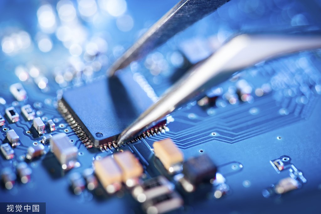
When designing PCBs, routing is essential. The quality of the routing affects the aesthetics, production cost, circuit performance, heat dissipation, and device optimization.
This article provides a comprehensive guide on PCB routing techniques:
1. The routing length should include the length of vias and solder pads.
2. The preferred routing angle is 135°. Arbitrary angles may cause manufacturing issues.

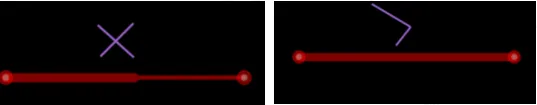
3. Avoid right angles or sharp corners, as they can cause impedance changes, signal reflection, and width variations at corners.

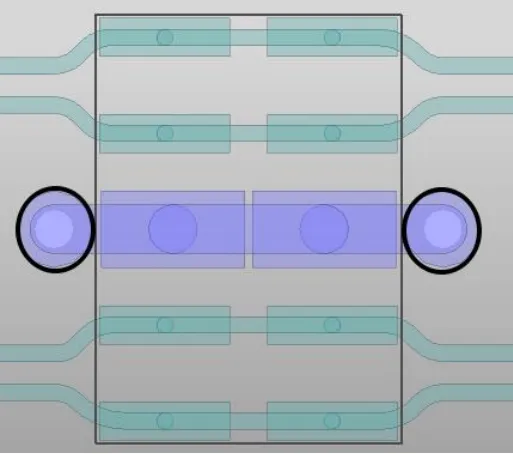
4. Routes should extend from the longer side of the pad. Avoid routing from the corners or wide sides, and ensure a clearance of more than 6 mils from the corner of the pad.

5. Adjacent pads in the same network should not be directly connected to avoid solder bridging during manual soldering.

6. For small CHIP components, maintain symmetrical routing with consistent width on both sides, especially for copper connections to prevent component displacement during placement.

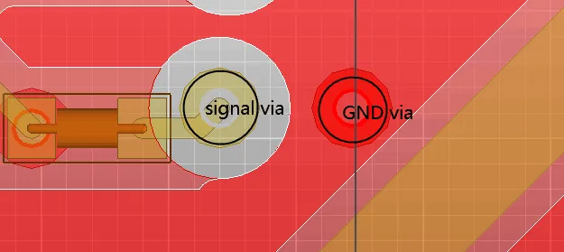
7. For signals requiring ground shielding, ensure continuous shielding and place GND vias close to each other, ideally 50-150 mils apart.

8. Ensure the routing has a complete and continuous reference plane and avoid crossing different regions for high-speed signals. Maintain at least 40 mils of clearance from the edge of the reference plane for high-speed signals.

9. To reduce impedance changes due to surface-mount pads, consider cutting out a section of the reference layer directly below the pad based on the pad size. Common surface-mount components include capacitors, ESD devices, common-mode inductors, connectors, etc.

10. Minimize the loop area formed by signal lines and their return paths, as smaller loops reduce radiation and external interference.

11. Avoid stub routing. Keep stub lengths as short as possible, ideally zero. Minimize via stubs to prevent affecting signal integrity, especially if the stub length exceeds 12 mils. Simulation can be used to evaluate the impact.


12. Avoid routing on different layers that form self-loops, which can lead to electromagnetic interference.

13. Do not place test points on high-speed signals.
14. For signals susceptible to interference (e.g., RF signals), use shielding. Shield width should be at least 40 mils, with many GND vias for effective soldering.

15. Keep the same network’s routing width consistent to avoid uneven characteristic impedance and potential signal reflections.
16. The width of IC pin routing should be less than or equal to the pad width. For wider signal traces due to current requirements, maintain the same width as the pad for about 6-10 mils before widening the trace.

17. All traces must connect to the center of the pads and vias.
18. Ensure sufficient creepage distance for high-voltage signals.
I. General AC-DC Power Supply (120VAC—240VAC)
| Description | Creepage Distance (mm) | Electrical Clearance (mm) |
| L to N | 3.2 before fuse | 2.5 before fuse |
| 2.5 after fuse | 2.0 after fuse | |
| Primary to Ground | 3.4 | 2.5 |
| Before Rectifier Bridge to After Bridge | 2.5 | 2.0 |
| F_before to F_after | 3.2 | 2.5 |
| MOS (Switch) to Ground | 4.0 | 2.8 |
| Primary to Secondary | 8.0 | 5.0 |
| Secondary to Ground | 1.4 | 0.7 |
II. AC-DC with PFC Circuit
| Description | Creepage Distance (mm) | Electrical Clearance (mm) |
| Primary to Ground | 4.5 | 2.7 |
| Primary to Secondary | 9.0 | 5.4 |
III. DC-DC Power Supply (60V—100V)
| Description | Creepage Distance (mm) | Electrical Clearance (mm) |
| Primary to Secondary | 3.5 | 2.0 |
| Primary to Ground | 1.8 | 1.0 |
| Before Fuse V+ to V- | 1.8 | 1.0 |
19. For designs involving multiple DDR or memory chips, confirm the routing topology with the customer and check for reference documentation.
20. Finger areas need full window processing, and copper layers beneath the finger area should be removed, maintaining a distance of at least 3 mm from the board frame.

21. Plan routing bottlenecks in advance, and optimize the narrowest sections.

22. Place decoupling capacitors as close to connectors as possible.
23. Place series resistors near the transmitting device and termination resistors near the end, such as the clock signal’s series resistor placed within 400 mils of the CPU.
24. For ICs like eMMC or FLASH, place a ground via near each ground pad to shorten return paths.

25. Place a ground via near each ESD device’s ground pad.
26. Avoid routing near clock components (e.g., crystals), switching power supplies, magnetic components, or plugin vias.
27. When changing signal layers, place a companion via next to the signal via for continuous return paths. For differential signals, ensure symmetrical placement of signal and return vias.

28. Ground copper around connectors should be at least three times the trace width from the signal pads.

29. For BGA areas with plane breaks, connect the plane with traces to maintain continuity.

30. For shielded traces, maintain at least 4*W distance between the trace and the shield and place ground vias at regular intervals.

31. For critical high-speed single-ended signals (e.g., clock and reset signals), add shielding with ground vias spaced every 500 mils.

The article is reprinted from the WeChat public account “21ic Electronics Network.” Source: Breadboard Community.

Choosing the Right Wires for Breadboard Wiring: A Comprehensive Guide
Breadboards are a staple in electronic circuit building, offering flexibility and ease of use for both beginners and professionals. However, one of the most critical aspects of working with breadboards is selecting the right wires. The wires you choose can impact not only the functionality of your circuit but also its longevity and ease of…

How to Improve Heat Dissipation in PCB Design
Introduction As modern electronic devices become more complex and power-dense, heat dissipation has emerged as a critical factor that directly impacts device performance and reliability. Excessive junction temperatures in electronic systems can shorten the lifespan of components and lead to system failure. Thus, optimizing the PCB (Printed Circuit Board) design to improve heat dissipation is…

Manufacturing Process of Multilayer PCBs
Multilayer PCB manufacturing methods include the plated-through hole (PTH) and high-density interconnect (HDI) methods, both achieved by combining different processes to realize the circuit board structure. Currently, the most widely used method is the PTH method, which has been developed and refined over more than half a century. The PTH method is mature in terms…